High- k gate dielectric GaAs MOS device with LaON as interlayer and NH3-plasma surface pretreatment
Liu Chao-Wen, Xu Jing-Ping† , Liu Lu, Lu Han-Han
, Liu Lu, Lu Han-Han 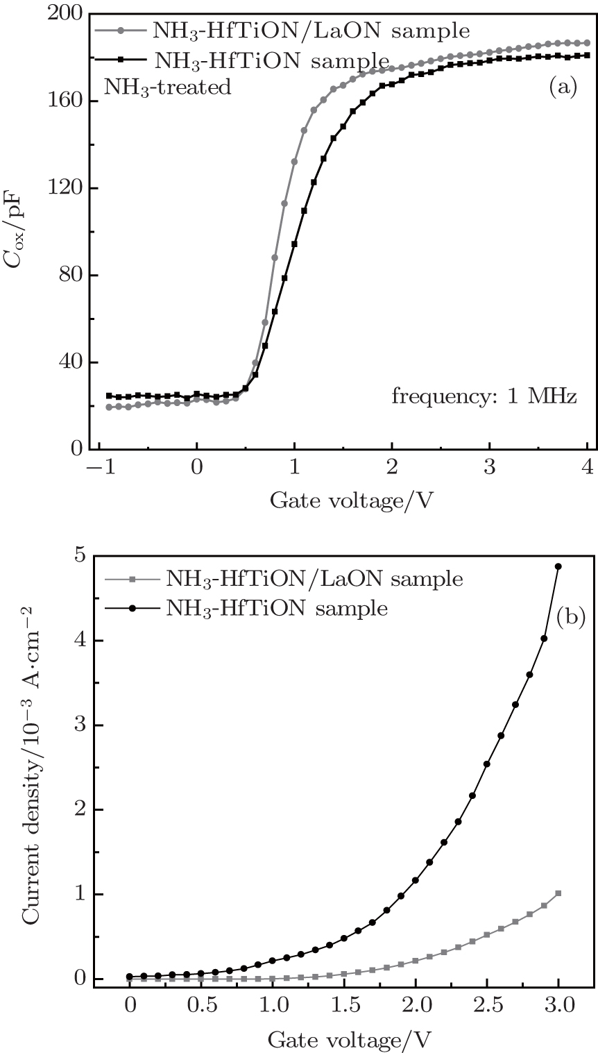
High- k gate dielectric GaAs MOS device with LaON as interlayer and NH3-plasma surface pretreatment |
|
Liu Chao-Wen, Xu Jing-Ping†
, Liu Lu, Lu Han-Han |
| HF C – V curves (a) and I – V characteristics (b) of the NH3-plasma treated samples with and without LaON IPL. |
| |