

High- k gate dielectric GaAs MOS device with LaON as interlayer and NH3-plasma surface pretreatment
[Liu Chao-Wen, Xu Jing-Ping† , Liu Lu, Lu Han-Han]
, Liu Lu, Lu Han-Han]
|
|


†Corresponding author. E-mail: jpxu@hust.edu.cn
*Project supported by the National Natural Science Foundation of China (Grant Nos. 61176100 and 61274112).
High- k gate dielectric HfTiON GaAs metal-oxide–semiconductor (MOS) capacitors with LaON as interfacial passivation layer (IPL) and NH3- or N2-plasma surface pretreatment are fabricated, and their interfacial and electrical properties are investigated and compared with their counterparts that have neither LaON IPL nor surface treatment. It is found that good interface quality and excellent electrical properties can be achieved for a NH3-plasma pretreated GaAs MOS device with a stacked gate dielectric of HfTiON/LaON. These improvements should be ascribed to the fact that the NH3-plasma can provide H atoms and NH radicals that can effectively remove defective Ga/As oxides. In addition, LaON IPL can further block oxygen atoms from being in-diffused, and Ga and As atoms from being out-diffused from the substrate to the high- k dielectric. This greatly suppresses the formation of Ga/As native oxides and gives rise to an excellent high- k/GaAs interface.
In recent years, III– V (e.g. GaAs)-based metal– oxide– semiconductor (MOS) devices with high-k gate dielectric have been intensively investigated. These studies are motivated by their application in high-speed circuits due to some of their inherent advantages, such as high carrier mobilities, large energy bandgaps, and low power consumption.[1, 2] However, it has been shown that the interface between high-k gate dielectric and GaAs semiconductor is usually of poor quality and a high interface-state density due to the formation of native oxides (Ga2O3, As2O3, and the mixture of As2O3 and As2O5) on the GaAs surface, thus leading to Fermi-level pinning.[3, 4] Therefore, suppressing the growth of the native oxides on the surface of GaAs has become a key factor to obtain excellent electrical properties. Some investigations have suggested that surface treatment methods, e.g. sulfur passivation by (NH4)2S, can effectively reduce the native oxide on the surface of GaAs.[5, 6] In addition, plasma has been widely used to passivate the interface between the high-k and semiconductor, e.g., N2-plasma[7, 8] and NH3-plasma[9– 11] treatments on the semiconductor surface directly. It was found that the N2- and NH3-plasma pretreatments can efficiently remove the volatile element As from the surface, and reduce the Ga– O and As– O bonds.[12] On the other hand, it is also important to select the high-k gate dielectric reasonably to improve the high-k/GaAs interface. As is well known, Hf-based oxide has attracted wide attention.[13] Ti oxide has a high k value, and nitrogen incorporated into HfTiO can further increase its k value and reduce oxide charges and border traps.[14] Therefore, the HfTiON is considered as a promising high-k gate dielectric for a GaAs MOS device. However, an interface layer should be inserted between HfTiON and GaAs substrate to improve their interface quality. Although La-based oxide has a high k value, large bandgap, it has enough conduction-band offset, and it has a small lattice mismatch with GaAs, [15] the moisture absorption of La-based oxide can lead to a stability problem.[16] Incorporation of N into La2O3 leading to the formation of LaON can increase its k value and maintain good interfacial property. On the other hand, the formation of a N-related strong bond at or near the LaON/GaAs interface can enhance the thermal stability and reliability of the device.[17] Naturally, it is feasible to use LaON as the interface passivation layer (IPL). So, taking the above various factors into consideration in this work, GaAs MOS devices with LaON as IPL and HfTiON as high-k layer as well as N2- or NH3-plasma surface pretreatment are fabricated. Their interfacial and electrical properties are then investigated and compared with their counterparts with neither LaON IPL nor surface treatment.
GaAs MOS capacitors were fabricated on the Si-doped n-GaAs (100) wafers with a doping concentration of 0.5 × 1018 cm− 3 ∼ 1 × 1018 cm− 3. The wafers were degreased sequentially in deionized water, acetone, alcohol, and isopropanol for 5 min, respectively. They were then dipped in diluted HCl to remove native oxides, followed by (NH4)2S dipping for 40 min to sulfur-passivate the surface of the wafers.
After drying by N2, the surfaces of wafers were subjected to N2- or NH3-plasma pretreatment in PECVD chamber at 350 ° C, with a gas flow rate of 4 sccm and a radio frequency (RF) power of 120 W. Then, an about 2-nm LaN was deposited on the surface of each wafer with N2- or NH3- plasma treatment as IPL by reactive RF-sputtering of La target (RF power of 54 W) in an Ar/N2 (15 sccm/6 sccm) ambient at room temperature with an operating pressure of 0.5 Pa. Next, an about 10-nm HfTiN as high-k layer was in-situ deposited by co-sputtering of Hf (RF power of 56 W) and Ti (DC power of 28 W) targets in the same ambient. The two samples are denoted as N2-HfTiON/LaON and NH3-HfTiON/LaON samples, respectively. To address the role of LaON IPL, a sample with NH3-plasma surface pretreatment but only HfTiON (∼ 12 nm) as gate dielectric was also prepared (which is denoted as the NH3-HfTiON sample). To address the role of the plasma pretreatment, a wafer without any plasma pretreatment was used to prepare the stacked gate dielectric of Hf- TiON/LaON as a control sample. Post-deposition annealing of all the samples was performed at 600 ° C for 60 s in N2 (500 sccm) + O2 (50 sccm) to transform LaN and HfTiN into LaON and HfTiON, respectively. Finally, Al was thermally evaporated and patterned as a gate electrode with an area of 7.85 × 10− 5 cm2 and also as the back electrode, followed by N2 annealing at 300 ° C for 20 min to reduce their contact resistance.
The high-frequency (HF, 1-MHz) capacitance– voltage (C– V) curve and gate leakage current density versus gate voltage (Jg– Vg) curves of the samples were measured with a HP4284A precision LCR meter and a HP4156A semiconductor parameter analyzer, respectively. The physical thickness of the gate dielectric was measured by spectroscopic ellipsometry. The chemical states at/near the high-k dielectric/GaAs interface were analyzed by x-ray photoelectron spectroscopy (XPS).
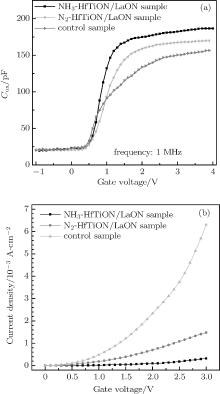
Figure 1 shows HF C– V curves and I– V characteristics of all the samples with LaON IPL. It can be seen that the control sample without surface pretreatment exhibits poor C– V behavior with largest “ stretch out” and smallest slope [see Fig. 1(a)], indicating a high density of interface states that are probably due to weak As– O, As– As, and Ga– O bonds at the GaAs/LaON interface.[4] However, the two plasma-treated samples, especially for the NH3-treated sample, show clear accumulation saturation and steep slope in depletion regime [Fig. 1(a)], implying less interface states and an unpinned Fermi level. The gate-oxide capacitance (Cox), flat-band voltage (Vfb), and interface- state density at midgap (Dit) are extracted from the HF C– V curves, where the Dit was extracted by Terman’ s method for comparison only, as listed in Table 1. The positive shift of Vfb indicates that negative charges exist in the dielectric film and at/near the interface, which are probably associated with acceptor-like interface states and nearinterface electron traps.[18] The values of Vfb are 0.78, 0.92, and 0.95 V for the NH3-HfTiON/LaON, N2-HfTiON/LaON, and control samples, respectively: the NH3-HfTiON/LaON sample has a smallest value. This happens because NH3- or N2-plasma pretreatment can incorporate nitrogen atoms onto the surface of GaAs to fill the oxygen vacancies. On the other hand, it can build a N barrier to block Ga and As atoms from being out-diffused from the substrate to the high-k dielectric.[19] This reduces the formation of Ga- and As-oxides and leads to less oxide charges and interface states, especially for the NH3-HfTiON/LaON sample due to more nitrogen incorporation at the surface of GaAs. In addition, the reductions of the interfacial Ga- and As-oxides can increase accumulation capacitance, which is more obvious for the NH3-HfTiON/LaON sample since the oxygen incorporated into the interface can be suppressed more effectively by the reactive species of H atoms and NH radicals from NH3-plasma.[11] The smaller Dit for the NH3-HfTiON/LaON sample than for the N2-HfTiON/LaON sample is also partly ascribed to the reactive species of H atoms and NH radicals, [10, 11] which could terminate the dangling bonds to some extent.
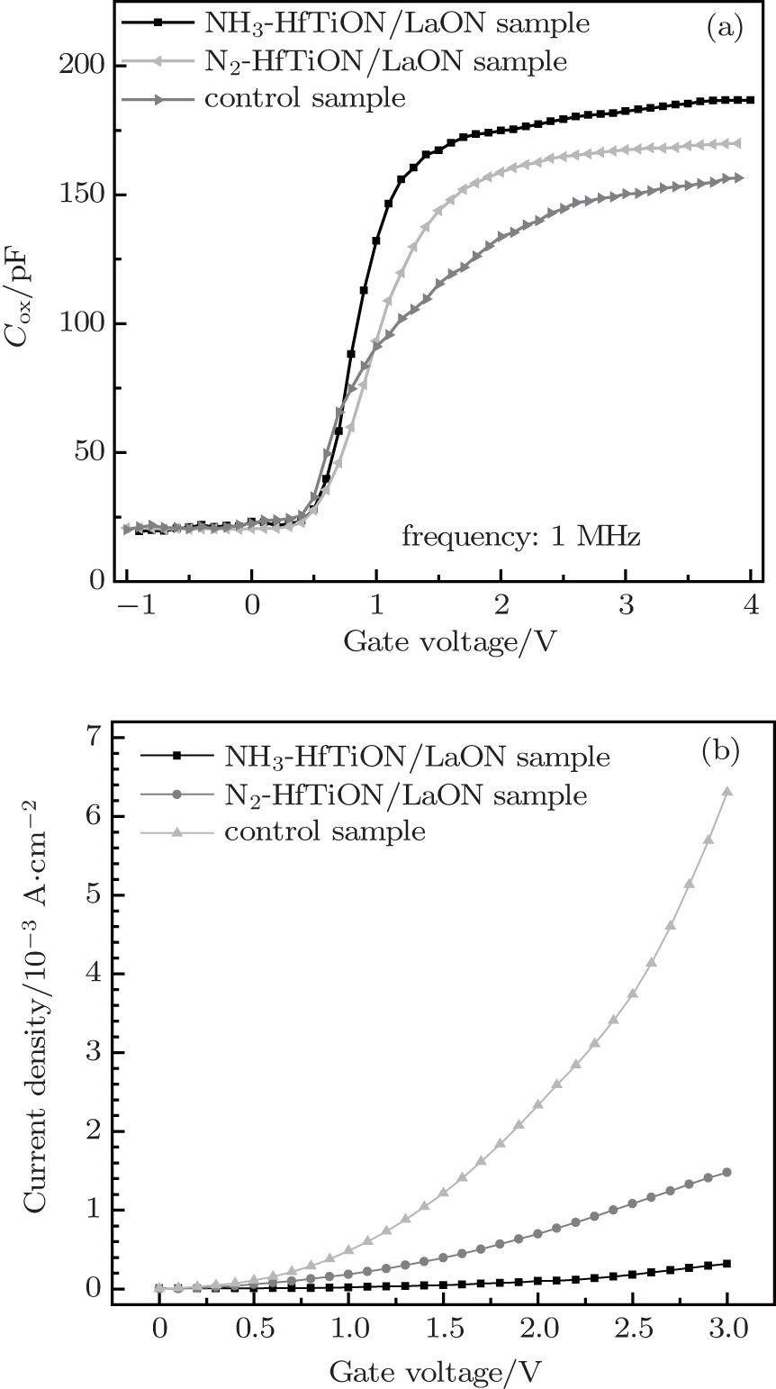 | Fig. 1. HF C– V curves (a) and I– V characteristics (b) of all the samples with LaON IPL. |
| Table 1. Electrical and physical parameters extracted from HF C– V curves for all the samples with LaON IPL. |
Moreover, as shown in Fig. 1(b), the NH3-HfTiON/LaON sample exhibits the smallest gate leakage current, followed by the N2-HfTiON/LaON and control samples in turn, i.e., 6.78× 10− 5 A/cm2, 6.31× 10− 4 A/cm2, and 2.076× 10− 3 A/cm2 at Vfb+ 1 V for the NH3-HfTiON/LaON, N2-HfTiON/LaON, and control samples, respectively. This is closely associated with magnitude of its Dit.
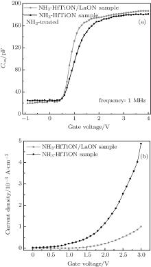
In order to clarify the role of LaON as IPL, the C– V and I– V characteristics of the NH3-plasma surface pretreatment samples with or without LaON IPL, i.e., the NH3- HfTiON/LaON and NH3-HfTiON samples, are measured and compared, as shown in Fig. 2. Obviously, the NH3-HfTiON sample exhibits poorer C– V curve and larger gate leakage current than the NH3-HfTiON/LaON sample, with Vfb values extracted from their C– V curves being 0.95 V and 0.78 V, respectively. In addition, the Dit value extracted from the C– V curve is smaller for the NH3-HfTiON/LaON sample (2.6× 10¹² eV− 1· cm− 2) than for the NH3-HfTiON sample (4.2× 10¹² eV− 1· cm− 2). This indicates that the LaON IPL can further suppress the growths of defective low-k interfacial Ga/As oxides by enhancing resistance to in-diffusion of oxygen and out-diffusion of Ga/As atoms, thus leading to an excellent high-k/GaAs interface quality.
 | Fig. 2. HF C– V curves (a) and I– V characteristics (b) of the NH3-plasma treated samples with and without LaON IPL. |
To identify the composition and chemical states of the gate dielectric and to further analyze the effects of NH3- and N2-plasma pretreatment on the LaON/GaAs interface properties, the HfTiON film is etched to a depth of ∼ 3 nm from the GaAs surface with an in-situ Ar+ ion beam for the XPS analysis. As can be seen in Fig. 3, the Ti 2p spectra of the NH3-HfTiON/LaON and N2-HfTiON/LaON samples display two main peaks at 456.2 eV and 461.8 eV, respectively. These are assigned to Ti 2p3/2 and Ti 2p1/2, in which the intensities of the two peaks are obviously weaker for the former than for the later. This indicates that the NH3-HfTiON/LaON sample can more effectively block the Ti atoms from diffusing onto the surface of GaAs substrate. A N 1s peak is detected in the inset of Fig. 3, indicating the presence of a nitrogen element in the interlayer and high-k layer. In Fig. 4 for the XPS spectra of Ga 3d, the peaks at 15.8 eV and 16.9 eV are due to Hf– N and Hf– O bonds. The peak located at 37.5 eV is from Ti– O bond, corresponding to Ti 3p3/2. The Hf 5p3/2 and Hf 5p1/2 peaks occur at 32.7 eV and 39.65 eV respectively, with Δ Hf 5p of ∼ 7 eV, [20] which are from Hf– O bonds. So, the formation of HfTiON dielectric is confirmed. Besides, the peaks at 16.4 eV and 17.6 eV are due to La– O and La– OH bands.[21] Considering the presence of O and N, LaON could be confirmed to exist at the GaAs surface. Thus, it can be suggested that the stacked gate dielectric of HfTiON/LaON is formed.
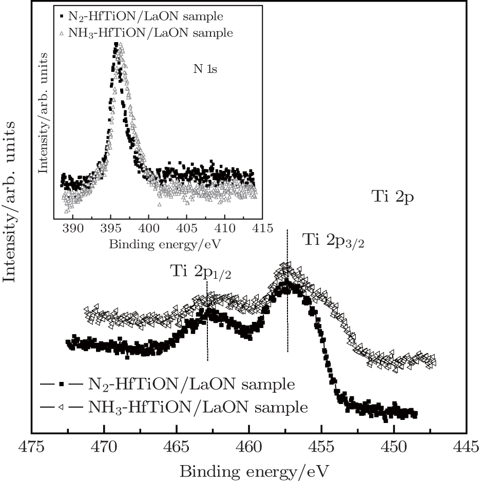 | Fig. 3. Ti 2p XPS spectra of the NH3-HfTiON/LaON and N2-HfTiON/LaON samples. |
 | Fig. 4. Ga 3d XPS spectra of the two plasma-treated samples with LaON IPL. (a) NH3-HfTiON/LaON sample and (b) N2-HfTiON/LaON sample. |
Furthermore, it can be seen from Fig. 4 that the Ga– O, Ga– S, and Ga– N peaks appear at 21.3 eV, 20.36 eV, and 19.43 eV, respectively. The percentages of the Ga-O/Ga-N bonds at the interface are calculated to be 11.94%/20.56% and 8.54%/28.88% for the N2-HfTiON/LaON and NH3-HfTiON/LaON samples respectively, based on the Ga– O/Ga3d or Ga– N/Ga3d peak area ratio. It is obvious that the percentages of the Ga– O/Ga– N bonds are lower/higher for the latter than the former. This indicates that the NH3-plasma pretreatment could more effectively reduce the weak Ga– O bonds and increase the strong Ga– N bonds than the N2 plasma because both of the species (e.g. N atoms and NH radicals) are provided by the NH3 plasma and supply of more N+ ions (since the NH3 plasma has lower ionization energy).[22]
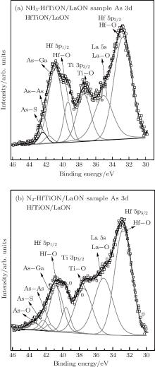
The XPS spectra of As 3d for the N2-HfTiON/LaON and NH3-HfTiON/LaON samples are shown in Fig. 5. From Fig. 5(b) for the N2-HfTiON/LaON sample, it can be seen that the As-O bond occurs at 43.42 eV, which disappears in Fig. 5(a) for the NH3-HfTiON/LaON sample. This indicates that the NH3-plasma treatment can also effectively remove the interfacial As oxide. This is why the NH3-HfTiON/LaON sample has better interface quality and electrical properties than the N2-HfTiON/LaON sample.
 | Fig. 5. As 3d XPS spectra of the two plasma-treated samples. (a) NH3-HfTiON/LaON sample and (b) N2-HfTiON/LaON sample. |
MOS capacitors with N2- or NH3-plasma surface pretreatment and LaON as IPL are fabricated, and their interfacial and electrical properties are investigated and compared with their counterpart with neither surface treatment nor LaON IPL. The experimental results show that the sample with LaON IPL and NH3-plasma pretreatment exhibits the improved C– V characteristic, lower gate leakage current density (6.78× 10− 5 A/cm2 at Vfb+ 1 V), and interface-state density (2.6× 10¹² eV− 1· cm− 2). The mechanisms involved lie in the fact that the NH3-plasma pretreatment can effectively remove the Ga/As native oxides due to the high-density species (e.g. H atoms and NH radicals). Furthermore, for the NH3-plasma pretreated samples, it is found that the sample with LaON as IPL has better interfacial and electrical characteristics that the sample without LaON IPL. This indicates that the LaON IPL can further suppress the growth of the native oxides.
| 1 |
|
| 2 |
|
| 3 |
|
| 4 |
|
| 5 |
|
| 6 |
|
| 7 |
|
| 8 |
|
| 9 |
|
| 10 |
|
| 11 |
|
| 12 |
|
| 13 |
|
| 14 |
|
| 15 |
|
| 16 |
|
| 17 |
|
| 18 |
|
| 19 |
|
| 20 |
|
| 21 |
|
| 22 |
|