
Material properties dependent on the thermal transport in a cylindrical nanowire
[Zhang Yonga) , Xie Zhong-Xiang†a)  , Deng Yuan-Xiang
a) , Yu Xia‡a) , Li Ke-Minb) ]
, Deng Yuan-Xiang, Li Ke-Min
 |


†Corresponding author. E-mail: xiezxhu@163.com
‡Corresponding author. E-mail: yuxia83@126.com
*Project supported by the National Natural Science Foundation of China (Grant No. 11404110), the Natural Science Foundation of Hunan Province, China (Grant Nos. 14JJ3139, 2015JJ6027, and 2015JJ6030), the Outstanding Young Program from the Education Department of Hunan Province, China (Grant No. 14B046), and the Doctoral Activation Foundation of Hunan Institute of Technology of China (Grant No. HQ14006).
Using the elastic wave continuum model, we investigate the effect of material properties on ballistic thermal transport in a cylindrical nanowire. A comparative analysis for the convexity-shaped and concavity-shaped structure is made. It is found that in the convexity-shaped structure, the material with higher wave velocity in the convexity region can increase the thermal conductance at the lower temperature range; the thermal conductance of the nanowire with higher wave velocity in the convexity region is lower than that of the nanowire with lower wave velocity in the convexity region at the higher temperature range. However, in the concavity-shaped structure, the material properties of the concavity region have less effect on the thermal conductance at the lower temperature range; the material with higher wave velocity in the concavity region can reduce the thermal conductance at the higher temperature range. A brief analysis of these results is given.
In recent years, thermal properties associated with acoustic phonons in semiconductor nanostructures have attracted a great deal of attention.[1– 8] Employing the Landauer formulation of transport theory, Rego et al.[9] firstly predicted the existence of thermal conductance quantization, 
In the present work, we investigate the effect of material properties on ballistic phonon transmission and thermal conductance in a cylindrical nanowire at low temperatures by applying the elastic wave continuum model method. To the best of our knowledge, only rectangular geometries are considered in previous studies. However, the thermal transport properties in a cylindrical semiconductor nanowire are paid very little attention. Generally, cylindrical structures can be used more widely in experimental measurement and potential applications compared to rectangular structures. Our results show that in the zero temperature limit, the quantum value 
This paper is organized as follows. In Section 2, we give a brief description of the model and the formulas used in calculations. In Section 3, we numerically discuss the phonon transmission coefficient and thermal conductance. Finally, we summarize our results in Section 4.
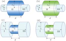
We consider the model structure shown in Fig. 1, a cylindrical semiconductor nanowire is connected by a scattering region with different materials. Here, we suppose that the temperatures in regions I and III are TL and TR, respectively. The temperature difference δ T (δ T = TL − TR) is so small that we can use the mean temperature T [T = (TL + TR)/2] as the temperature of region I and III in the following calculation. The formula of thermal conductance in the ballistic region can be written as:[26]

where ω m is the cutoff frequency of the m-th mode; β = 1/(kBT), where kB and T are the Boltzmann constant and temperature, and ħ is Planck’ s constant, respectively. τ m(ω ) is the energy transmission coefficient of the m-th mode at frequency ω from region I across all the interfaces into region III, which is the key issue to calculate τ m(ω ).
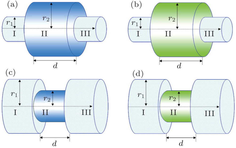 | Fig. 1. Schematic diagram for two semi-infinite cylindrical nanowires with an embedded abrupt scattering region made of different materials. Panels (a) and (b) correspond to the convexity-shaped structure with GaAs and AlAs convexity region, panels (c) and (d) correspond to the concavity-shaped structure with GaAs and AlAs concavity region, respectively. |
At low temperatures, ballistic phonon wavelengths are generally over several hundreds of angstroms, which are much greater than the dimensions of the structure. Naturally, microscopic length such as the atomic bond length is much smaller than the wavelength of the ballistic phonon. Thus, we use the elastic wave continuum model to describe the ballistic phonon propagation in this work. In the elastic approximation, the phonon displacement U(r, θ , z) in the cylindrical coordinate satisfies the following equation:

where 
where 


Here, Jn is the n-th-order Bessel function of the first kind, and χ m is the m-th solution of J2(χ m) = 0. Then we can calculate the transmission coefficient τ m by using the scattering matrix method. In the calculations, we take all the propagating modes and several lowest evanescent modes into account to meet the desired precision. For further details of these calculations, see Li et al.[35]
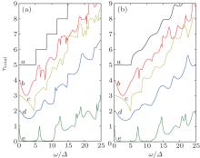
In Fig. 2, we calculate the total transmission coefficient τ total as a function of the reduced frequency ω /Δ (Δ = v/r1) for varying radii r2 of the scattering region with different materials. Here, the material in regions I and III is always GaAs. For comparison, the transmission coefficient for an ideal nanowire is also calculated in Fig. 2(a). From the figure, we can find that the τ total curve shows ideal quantum transmission stepwise platforms that gives the number of the phonon transport channels in the ideal nanowire, indicating that the available phonons can pass completely through this structure without reflection. Note that the breadth of these platforms is nonuniform especially for the first platform, which is different from that in rectangular nanowires.[36] When the material GaAs in region II is substituted by AlAs in a straight nanowire, from Fig. 2(b), τ total decreases strongly from interface scattering of incident phonons from the acoustic mismatch, the ideal transmission coefficient is destroyed and becomes blurred especially when the reduced frequency ω /Δ is larger than 5. In the presence of the abrupt scattering region in region II, the transmission coefficient further reduces due to the added scatter by the discontinuous abrupt interfaces in Fig. 2.
 | Fig. 2. Total transmission coefficient τ total as a function of the reduced frequency ω /Δ for different radii r2. Panel (a) corresponds to the scattering region with material GaAs and panel (b) corresponds to the scattering region with material AlAs. Curves a, b, c, and e are for r2 = 10, 15, 12, 8, and 5 nm, respectively. Here, we take r1 = 10 nm and d = 5 nm. Each curve is vertically offset by unity for clarity. |
In the concavity-shaped structure, the transmission coefficient significantly decreases. In the limit ω → 0, however, all the τ total values remain unity regardless of the geometric parameters and material properties of the scattering region. This can be well understood, the phonon wavelength λ depends on the material wave velocity υ and the phonon frequency ω , which can be expressed as λ = 2π υ /ω . Here, wave velocity υ is a constant, thus the wavelength λ increases as the phonon frequency ω decreases, meaning that a phonon with extremely long wavelength at ω = 0 is hardly scattered by the discontinuous interfaces. Note that, at r2 = 5 nm, in the low-frequency region, the total transmission coefficient exhibits some stop-frequency gaps, which can be opened and are clearly different from these stemming from the Van Hove singularities of perfect phonon bands. These stop-frequency gaps may be attributed to the antiresonant coupling between the incident waves and reflected waves because of multi-reflection in the scattering region. As the incident frequency increases (ω /Δ > 6), the stepped profile of the transmission coefficient becomes more distinct, and the number of transmission platforms increases. To understand these behaviors, the cutoff frequency, ω m = χ mv/r2, needs to be analyzed. When the incident frequency is larger than the cutoff frequency of the m-th mode, this mode can be excited to contribute to the phonon transmission. As r2 increases, ω m decreases, so more modes can be excited. Thus, the number of the excited modes in the convexity-shaped structure is larger than that in the concavity-shaped structure.
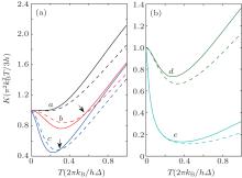
Now, we turn to investigate how the phonon thermal conductance depends on the reduced temperatures and structural parameters. In Fig. 3, we depict the total thermal conductance K as a function of the reduced temperature T for different radii r2. For the straight cylindrical nanowire (r2 = 10 nm), K presents the longer quantum platform in the low temperature range compared to the rectangular nanowire.[36] As the temperature goes up, higher index phonon modes are excited and contribute to the thermal conductance, thus thermal conductance increases monotonously. It is worth pointing out that due to the higher cutoff frequencies in cylindrical nanowires, the magnitude of thermal conductance in cylindrical nanowires is always smaller than the corresponding value in rectangular nanowires at high temperatures.[36] When the abrupt scattering region is emerged in the nanowire, the thermal conductance curve descends markedly due to sudden material and structural changes from the quantum value to a minimum at low temperatures. However, in the limit T → 0, K approaches the universal value 
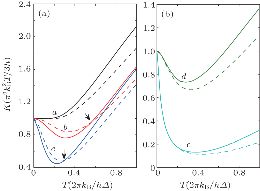 | Fig. 3. Total thermal conductance K as a function of the reduced temperature kBT/ħ Δ for different radii r2. Curves a, b, c, d, and e are for r2 = 10, 12, 15, 8, and 5 nm, respectively. Solid and dashed curves correspond to the scattering region with material GaAs and AlAs, respectively. The other geometrical parameters are identical to those in Fig. 2. |
In order to further reveal the thermal conductance properties, in Fig. 4, we show the thermal conductance for the individual modes as a function of the reduced temperature for different radii r2. Figures 4(a), 4(b), and 4(c) correspond to the modes m = 0, 1, and 2, respectively. It is clearly seen that, for each r2, the thermal conductance reduces as the modal index m increases. This can help explain why only several lowest modes can contribute to the thermal conductance at low temperatures. For the higher modes, their thermal conductance rapidly increases from the zero as the temperature increases. However, the thermal conductance is usually smaller than that of the zero mode, even at higher temperatures. These behaviors indicate that the zero mode plays an important role in determining phonon thermal conductance at low temperatures.
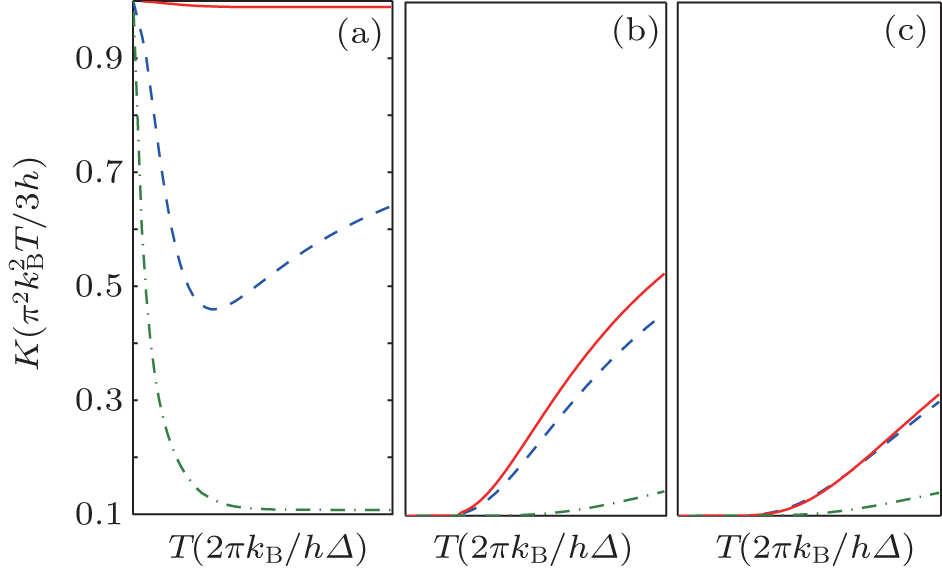 | Fig. 4. The thermal conductance K for the three lowest modes as a function the reduced temperature kBT/ħ Δ for different radii r2 of the scattering region with AlAs material. Panels (a), (b), and (c) correspond to the modes m = 0, 1, and 2. Solid, dashed, and chain curves correspond to r2 = 10 nm, 15 nm, and 5 nm, respectively. The other geometrical parameters are identical to those in Fig. 2. |
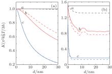
Finally, figure 5 shows the total thermal conductance K as a function of the length d of the scattering region at the temperature controlled area. The results show that, at very low temperatures, T = 0.2 K, the total thermal conductance is 

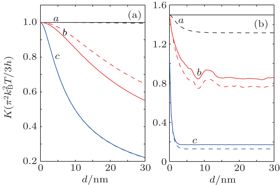 | Fig. 5. Total thermal conductance K as a function of the length d of the scattering region for different radii r2 at the temperature controlled area. Panels (a) and (b) correspond to T = 0.2 K and T = 2 K. Curves a, b, and c are for r2 = 10, 15, and 5 nm, respectively. Solid and dashed curves correspond to the scattering region with material GaAs and AlAs. Here, we take r1 = 10 nm. |
We have investigated material properties dependent on the thermal transport in a cylindrical semiconductor nanowire by using the elastic wave continuum model. Our numerical results show an interesting physical effect: the behavior of the thermal conductance is different for different types of the scattering region with different types of the material. In the convexity-shaped structure, the material with higher wave velocity in the convexity region can increase the thermal conductance at the lower temperature range; the thermal conductance of the nanowire with higher wave velocity in the convexity region is lower than that of the nanowire with lower wave velocity in the convexity region at the higher temperature range. However, in the concavity-shaped structure, the material properties of the concavity region have less effect on the thermal conductance at the lower temperature range; the material with higher wave velocity in the concavity region can reduce the thermal conductance at the higher temperature range. Moreover, a quantized thermal-conductance plateau can be observed in an ideal cylindrical nanowire. To further study how the scattering region affects the thermal conductance properties, we also studied the individual mode and found that the zero mode plays an important role in determining phonon thermal conductance at low temperatures. Our results suggest that adjusting the structure and material properties of the scattering region may provide a valuable reference for modulating thermal transport in application of nanoscale devices.
| 1 |
|
| 2 |
|
| 3 |
|
| 4 |
|
| 5 |
|
| 6 |
|
| 7 |
|
| 8 |
|
| 9 |
|
| 10 |
|
| 11 |
|
| 12 |
|
| 13 |
|
| 14 |
|
| 15 |
|
| 16 |
|
| 17 |
|
| 18 |
|
| 19 |
|
| 20 |
|
| 21 |
|
| 22 |
|
| 23 |
|
| 24 |
|
| 25 |
|
| 26 |
|
| 27 |
|
| 28 |
|
| 29 |
|
| 30 |
|
| 31 |
|
| 32 |
|
| 33 |
|
| 34 |
|
| 35 |
|
| 36 |
|