Strictly non-blocking 4×4 silicon electro–optic switch matrix
[Zhou Pei-Ji, Xing Jie-Jiang, Li Xian-Yao, Li Zhi-Yong, Yu Jin-Zhong, Yu Yu-De† ]
]
]
|
|


†Corresponding author. E-mail: yudeyu@semi.ac.cn
*Project supported by the National Basic Research Program of China (Grant No. 2011CB301701), the National High Technology Research and Development Program of China (Grant Nos. 2013AA014402, 2012AA012202, and 2015AA016904), and the National Natural Science Foundation of China (Grant Nos. 61275065 and 61107048).
The first path-independent insertion-loss (PILOSS) strictly non-blocking 4×4 silicon electro–optic switch matrix is reported. The footprint of this switch matrix is only 4.6 mm×1.0 mm. Using single-arm modulation, the crosstalk measured in this test is –13 dB∼ –27 dB. And a maximum crosstalk deterioration of 6dB caused by two-path interference is also found.
Owing to the demand of bandwidth and capacity continuing to rapidly increase, communication systems are required to have higher performances.[1] Optical switches are becoming more and more important in future high-speed switching networks.[2, 3]
Strictly non-blocking switches, rearrangeable nonblocking switches, and blocking switches are three kinds of switch networks. A strictly non-blocking switch network is an ideal switch matrix. Its main advantage is that a new optical path is rebuilt without interrupting other optical paths, with the optical path allocation controlled by a simple algorithm. In a practical optical network, because the demand of the bandwidth and capacity keeps increasing, blocking has a very serious effect on network performance.
A strictly non-blocking matrix has many types of topological structures, like crossbar topology, [4] tree topology, [5] and path-independent insertion-loss (PILOSS) topology.[6– 8] Compared with other topological structures, the PILOSS topological structure needs fewer intersections. And also the topological structure is simple and extensible. For these reasons, this topological structure is believed to be the most promising for the future.
Silicon photonics provides a promising platform to achieve efficient, mass-producible and hence low-cost, highly integrated, and small-footprint optical devices. Silicon electro– optic switches, which are compatible with commercial complementary metal– oxide semiconductors (CMOS), provide an effective method for future high-speed network switching.[9– 11]
In this paper, a PILOSS strictly non-blocking 4× 4 silicon electro– optic switch matrix is proposed, fabricated and characterized. Strictly non-blocking silicon thermal– optic switch matrices have been reported previously.[12, 13] However, to the best of our knowledge, this is the first strictly non-blocking 4 × 4 silicon electro– optic switch matrix that has been reported. The best state we measured is shown in Fig. 1(a). The crosstalk of this state is − 13 dB∼ − 24 dB, and the insertion loss is − 16 dB∼ − 20 dB.
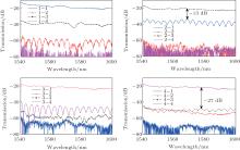
 | Fig. 1. (a) Schematic drawing of the strictly non-blocking 4× 4 switch matrix with a PILOSS network and the state we measured. (b) Microscope view of the fabricated strictly non-blocking 4× 4 switch matrix. |
Figure 1 shows the schematic drawing and the microscope view of the switch matrix with a PILOSS network. It consists of 16 electro– optic switching elements and 9 intersections. Under ideal conditions, the insertion loss (IL) in each of the switching elements is regarded as being the same. In fact, the ILs are not the same due to errors in fabrication, and this will cause a little difference in IL among paths.
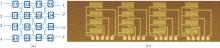
A 2× 2 symmetric Mach– Zehnder interferometer (MZI) structure is used in each switching element to achieve a large bandwidth, [14– 16] which includes two 2-port multimode interference (MMI) couplers and two symmetric modulation arms, one of which contains a 400-μ m-long PIN diode as shown in Fig. 2(a).
 | Fig. 2. (a) Schematic view of a commonly used 2× 2 Mach– Zehnder interferometer (MZI) switch. (b) Cross section view of an implemented p– i– n phase shifter. (c) The principle of electro– optic switch matrix. |
As shown in Fig. 2(b), the waveguide is 500-nm wide and 220-nm high with a 2-μ m-thick buried oxide layer. A 90-nm-thick slab is etched for single quasi-TE mode operation, which is fabricated by ultraviolet lithography. The PIN structure is realized by p-type and n-type doping each with a concentration of 1× 1019 cm− 3, with a doping region 500-nm away from the edge of the rib waveguide, and the electrodes are formed by depositing an aluminum layer. The final footprint of the switch matrix is 4.6 mm × 1.0 mm.
The principle of the electro– optic switch matrix is based on the free carrier dispersion (FCD) effect and Mach– Zehnder interferometer. When the PIN structure is at positive bias, the carrier concentration increases sharply. And this will cause the refractive index to decrease because of the FCD effect. The phase shift of one modulation arm is nkl, where n is the refractive index, k is the wave vector of the signal light in a vacuum, and l is the length of the modulation arm. The values of k and l are the same in the two modulation arms, but the values of n are not the same in the two modulation arms while one of the modulation arms is at positive bias. This makes phases different in the two arms. As shown in Fig. 2(c), when the phase difference between the two arms is 2kπ , this represents the cross state; when the phase difference between the two arms is (2k + 1)π , this refers to the bar state, where k is an integer. So the light intensity in the output can be changed by changing the voltage on the modulation arm.
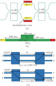
Before measuring a switch matrix, the electrical drive is applied to each of the 16 switching elements to reach the cross state and the bar state. The electrical drive for each switching element is shown in Table 1. The bold words represent the measurement values obtained under the condition of the best state. The measured transmission spectra of the best state from the four output ports of the switch matrix are shown in Fig. 3, which correspond to the routing states 1– 1′ , 2– 3′ , 3– 2′ , and 4– 4′ , and the crosstalk of − 13 dB∼ − 27 dB and the insertion loss of − 16 dB∼ − 20 dB are obtained. The crosstalk of the switch matrix is a little higher than that of the switching element.[17] The performance of the switch matrix can be improved in the future by adopting better switching elements and a better network design. In addition, obvious oscillations are found in these transmission spectra, like the spectrum between port 3 and port 4′ (3– 4′ ), which is caused by multiple-path interference. In particular, for two-path interference, this will cause maximum crosstalk to deteriorate by 6 dB. And in the switch matrix, a switching time of about 2 ns is finally realized under an electrical square wave driving signal with a frequency of 50 MHz.
 | Fig. 3. Measured transmission spectra from the four output ports of the switch matrix. |
| Table 1. Electrical drive for each switching element. |
In this work, the first PILOSS strictly non-blocking 4 × 4 silicon electro– optic switch matrix is proposed, fabricated and characterized. Using single-arm modulation, a crosstalk of − 13 dB∼ − 27 dB and an insertion loss of − 16 dB∼ − 20 dB are measured here. In addition, a maximum crosstalk deterioration of 6 dB, caused by two-path interference, is found in this paper.
| 1 |
|
| 2 |
|
| 3 |
|
| 4 |
|
| 5 |
|
| 6 |
|
| 7 |
|
| 8 |
|
| 9 |
|
| 10 |
|
| 11 |
|
| 12 |
|
| 13 |
|
| 14 |
|
| 15 |
|
| 16 |
|
| 17 |
|