Fin width and height dependence of bipolar amplification in bulk FinFETs submitted to heavy ion irradiation
Yu Jun-Tinga)  , Chen Shu-Ming
a), b) , Chen Jian-Juna) , Huang Peng-Chenga)
, Chen Shu-Ming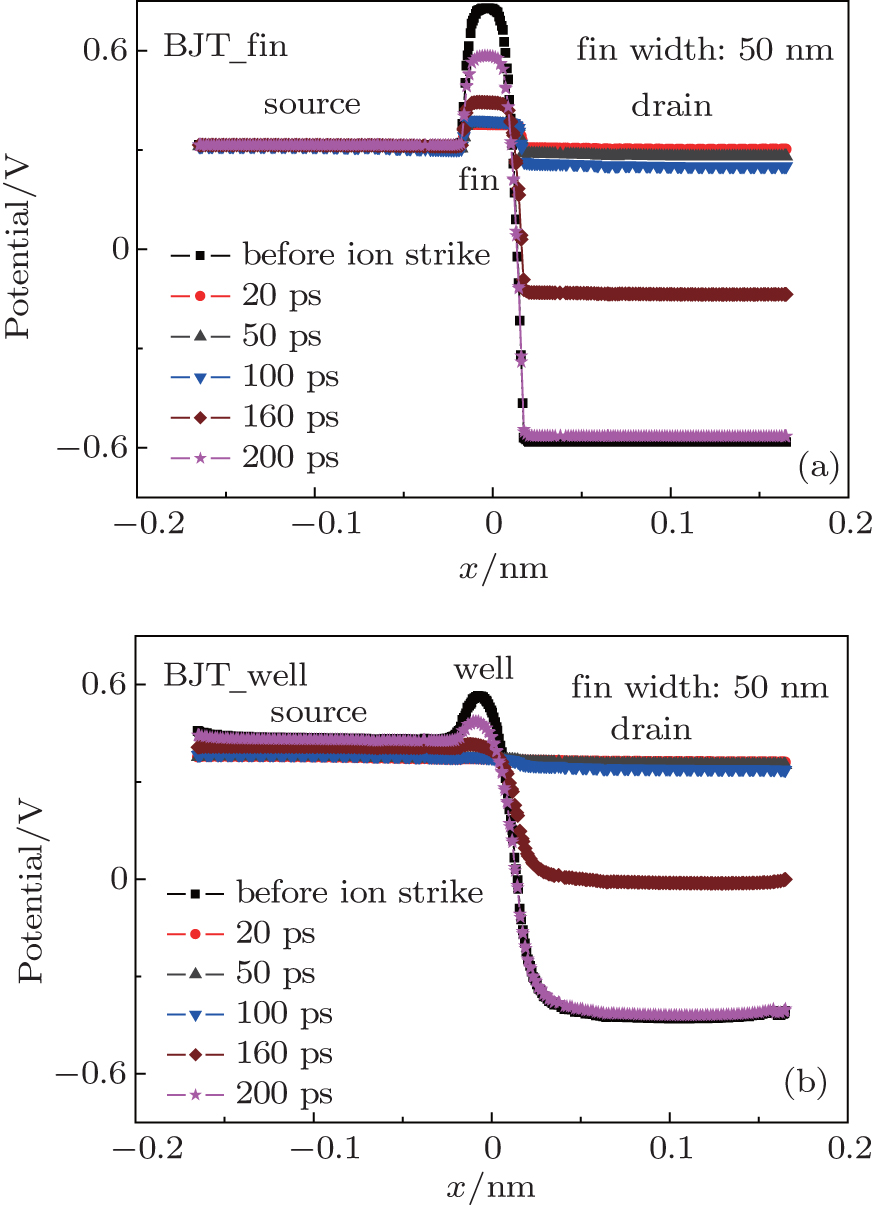
Fin width and height dependence of bipolar amplification in bulk FinFETs submitted to heavy ion irradiation |
|
Yu Jun-Ting
, Chen Shu-Ming |
| Potential profiles in 50-nm fin-width FinFET at different times before and after ion strike. (a) A cut line along the source-fin-drain ( x axis). (b) A cut line along the source-well-drain ( x axis), which are shown in Fig. 5 as white dot lines, 20 nm above and below the bottom of source/drain region, respectively. The ion LET is 10 MeV·cm2/mg. |
| |