Fin width and height dependence of bipolar amplification in bulk FinFETs submitted to heavy ion irradiation
Yu Jun-Tinga)  , Chen Shu-Ming
a), b) , Chen Jian-Juna) , Huang Peng-Chenga)
, Chen Shu-Ming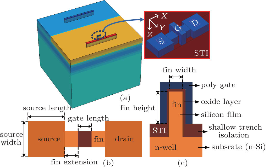
Fin width and height dependence of bipolar amplification in bulk FinFETs submitted to heavy ion irradiation |
|
Yu Jun-Ting
, Chen Shu-Ming |
| (a) 3D TCAD structure of the bulk p -FinFET. (b), (c) Top and cross-section views of FinFET, showing the gate length, fin width, and height of the device schematically, which are cut along the X – Y and Y – Z planes, respectively. The inset shows a zoomed view of the p -FinFET structure. |
| |