


Fin width and height dependence of bipolar amplification in bulk FinFETs submitted to heavy ion irradiation*
[Yu Jun-Tinga)  , Chen Shu-Ming
a), b) , Chen Jian-Juna) , Huang Peng-Chenga) ]
, Chen Shu-Ming|
|


†Corresponding author. E-mail: yjting nudt@163.com
*Project supported by the National Natural Science of China (Grant No. 61376109).
FinFET technologies are becoming the mainstream process as technology scales down. Based on a 28-nm bulk p-FinFET device, we have investigated the fin width and height dependence of bipolar amplification for heavy-ion-irradiated FinFETs by 3D TCAD numerical simulation. Simulation results show that due to a well bipolar conduction mechanism rather than a channel (fin) conduction path, the transistors with narrower fins exhibit a diminished bipolar amplification effect, while the fin height presents a trivial effect on the bipolar amplification and charge collection. The results also indicate that the single event transient (SET) pulse width can be mitigated about 35% at least by optimizing the ratio of fin width and height, which can provide guidance for radiation-hardened applications in bulk FinFET technology.
With technology scaling beyond 28-nm node, traditional planar transistors are vulnerable to undesirable short channel effects (SCEs), which present the most important constraints to MOSFET scaling rules. Owing to an enhanced electrostatic control on the silicon fin provided by the additional lateral gates, [1, 2] fin field effect transistor (FinFET) devices are regarded as the most promising candidates to continue CMOS scaling. As a consequence, FinFET technologies are currently becoming the mainstream process in the leading semiconductor manufacturers.[3]
Single event upset (SEU) is one of the most important issues with FinFET SRAM cells due to the smaller dimension and operating voltage of these devices.[4] A critical collected charge of only about 1.15 fC was reported to cause the upset event in a 6-T bulk FinFET SRAM.[5] Hence, it is highly significant to reduce the charge collection in scaled FinFET devices. As in planar devices, parasitic bipolar amplification can also play a key role in the charge collection of bulk and SOI FinFETs.[6– 11] It has been shown that device scaling affects the geometry of the fin, [1] and this can bring about an important impact on the bipolar amplification in FinFET transistors. Much work has been done to investigate the bipolar amplification of SOI FinFETs.[12– 17] However, the studies on bulk FinFETs are reported seldomly.
In this work, we have investigated the fin width (Wfin) and fin height (Hfin) dependence of heavy-ion-induced bipolar amplification in 28-nm bulk p-FinFETs with 3D TCAD numerical simulation. Simulation results show that the bipolar amplification of wider FinFETs is higher than that of the narrower ones, while the fin-height variations have a trivial effect on the bipolar amplification of bulk FinFETs. Besides, the narrower FinFETs also exhibit a reduction of SET pulse width about 35% at least. This gives a good indication that FinFETs with smaller fin width are more likely to exhibit higher tolerance to single event effects (SEEs). The rest of this paper is organized as follows. Section 2 presents the TCAD simulation setup and device structure. Section 3 shows the simulation results. Section 4 discusses the impact of fin width and fin height on bipolar amplification. Finally, the conclusions are given in Section 5.
Synopsys Sentaurus TCAD H-2013.03-SP1 is employed to investigate the effect of fin width and fin height on bipolar amplification of bulk p-FinFET devices. Figure 1 shows the 3D TCAD bulk p-FinFET structure and the corresponding geometrical parameters, which are developed with Sentaurus structure editor (SDE). For the simulated p-FinFET devices, the gate oxide is 1.2 nm thick and the gate work function used is a default value (4.9 eV for p-Si). The doping profile in the fin extension (the silicon finger between the gate edge and the source/drain regions, which is also called the source/drain access region) is the same as the highly doped source/drain regions (1020 cm− 3). The peak doping levels in the fin and n-well are 1018 and 1017 cm− 3, respectively. The FinFET device is calibrated with reference to the I– V characteristics of planar device in the 28-nm process.
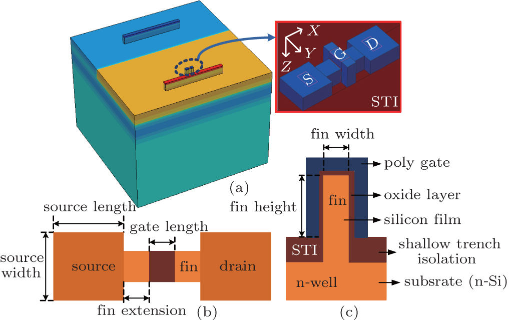 | Fig. 1. (a) 3D TCAD structure of the bulk p-FinFET. (b), (c) Top and cross-section views of FinFET, showing the gate length, fin width, and height of the device schematically, which are cut along the X– Y and Y– Z planes, respectively. The inset shows a zoomed view of the p-FinFET structure. |
As illustrated in Fig. 2, the bulk p-FinFET device is biased in the off-state during irradiation, that is, the drain is connected to the drain of an on-state NMOS configured with a SPICE model, while the source, gate, and n-well contacts are biased at supply voltage Vdd. The fin width, fin height, and other parameters considered in this paper are summarized in Table 1. Lgate and Weff are the gate length and effective width of FinFET device, respectively. As defined in Ref. [18], the effective width of FinFET is given by

where Nfin is the number of fins. In the simulations, all devices have only one fin, and the following physical models are used: 1) Fermi– Dirac carrier statistics; 2) band-gap narrowing effect; 3) doping-dependent Shockley– Read– Hall (SRH) and Auger recombination; 4) temperature, doping, electric field, and carrier– carrier– scattering impact on mobility; 5) a hydrodynamic model is used for the carrier transportation equations; and 6) incident heavy ions are modeled using a Gaussian radial profile with a characteristic 1/e radius of 50 nm and a Gaussian temporal profile with a characteristic decay time of 0.25 ps.
 | Fig. 2. Schematic configuration of the p-FinFET model in simulation, which is cut in the middle of the gate along the source/drain direction. |
| Table 1. Geometry variations in bulk p-FinFETs. |
All simulations are conducted for normal strike on the drain center of the devices with the ion linear energy transfer (LET) of 10 MeV· cm2/mg. In order to gain more insight into the influence of the source on the efficiency of the drain charge collection, the corresponding diode devices without source and gate terminals are also simulated. The collected charge is given by the drain current integration over the transient duration and the bipolar amplification is calculated as the ratio of charge collection between the FinFET and diode devices.[19]
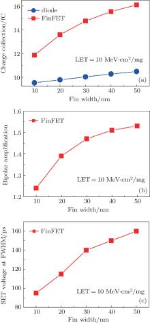
In order to investigate the fin-width dependence of bipolar amplification in bulk p-FinFETs, the Hfin is fixed at 50 nm, and devices with different Wfin ranging from 10 nm to 50 nm are simulated.
The results are shown in Fig. 3. It can be seen that the charge collection in FinFETs increases evidently when the fin width increases from 10 nm to 50 nm, almost by 36%. Correspondingly, the charge collection in diode devices increases slowly by less than 10%. As a result, the bipolar amplification in FinFETs increases from 1.24 to 1.53 and the SET voltage at the full width at half maximum (FWHM, which is also called pulse width) increases from 95 ps to 160 ps as the fin width ranges from 10 nm to 50 nm.
 | Fig. 3. (a) The amount of charge collection in FinFET and diode devices with different fin widths; (b) corresponding bipolar amplification for different fin-width FinFETs; (c) the SET voltage at FWHM for different fin-width FinFETs. All simulations are conducted with the same ion LET at 10 MeV· cm2/mg. |
Devices with different Hfin are simulated to explore the effect of fin height on the bipolar amplification of bulk p-FinFETs. In the simulations, the fin width is fixed at 20 nm, and the fin height increases from 35 nm to 55 nm.
The results are shown in Fig. 4. The charge collection of FinFET and diode devices increases slowly with the fin height increasing from 35 nm to 55 nm. Thus, the bipolar amplification increases from 1.38 to 1.41, which indicates that the fin height has little effect on bipolar amplification of FinFET. Besides, the SET voltage at FWHM increases from 105 ps to 120 ps as the fin height varies from 35 nm to 55 nm, which also verifies the contribution of bipolar amplification on SET pulse width.
 | Fig. 4. (a) The amount of charge collection in FinFET and diode devices with different fin heights. (b) The corresponding bipolar amplification for different fin-height FinFETs. (c) The SET voltage at FWHM for different fin-height FinFETs. All simulations are conducted with the same ion LET at 10 MeV· cm2/mg. |
After the last section, the bipolar amplification of bulk p-FinFET is independent of fin height, but strongly dependent on fin width. Figure 5 depicts the current curves and the charge collected versus time captured at the drain/source terminals for a 50-nm fin-width FinFET after the ion strikes with an LET of 10 MeV· cm2/mg. As shown in Fig. 5(a), there is obvious source injection current, which proves that the bipolar amplification has an important effect on the SET current and charge collection in bulk FinFET.
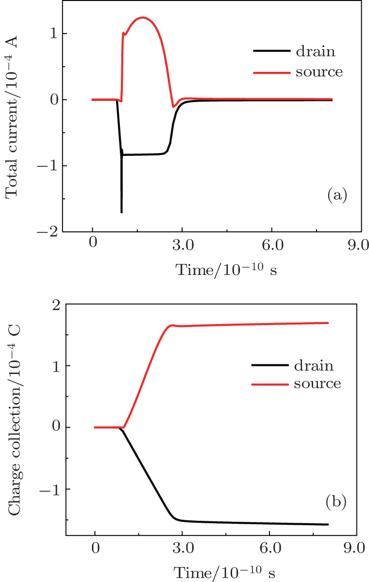 | Fig. 5. (a) Current curves captured at the drain/source terminals in a 50-nm fin-width FinFET. (b) The corresponding charge collection versus time for the drain/source terminals. The ion LET is 10 MeV· cm2/mg. |
In order to gain more insight into the bipolar amplification mechanism, the action of parasitic bipolar junction transistors (BJTs) in the devices is studied in detail. As shown in Fig. 6, two parasitic bipolar junction transistors (BJTs) exist in bulk p-FinFET. Generally, the source, drain, and n-well/channel (fin) in FinFET act as the emitter, collector, and base of BJTs, respectively. According to the location of the base, the BJT with the base in n-well is called BJT_well, while the BJT with the base in fin is called BJT_fin. The open of two BJTs depends on the n-well potential variation and fin potential variation, respectively, which is analyzed later.
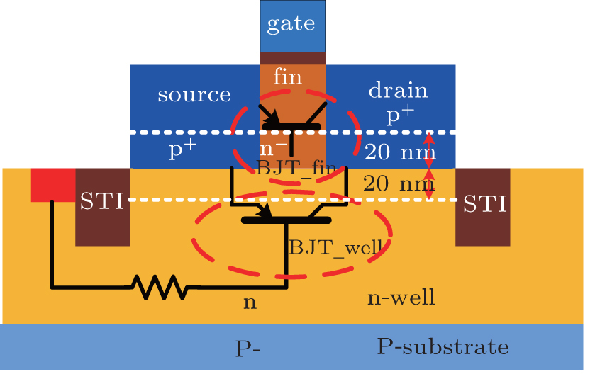 | Fig. 6. Parasitic bipolar junction transistors (BJTs) in bulk p-FinFET. |
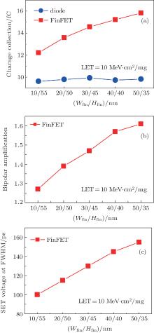
As shown in Fig. 7, the potential in 50-nm fin-width FinFET varies with time evidently. In BJT_fin, the potential barrier between source (emitter) and fin (base) always exits during a single event. However, in the BJT_well, when the ion strikes the FinFET, the excess of generated electrons in the well can disturb the well potential. As time goes on, the potential barrier disappears after the ion strikes. It indicates that the holes from the source pole are easier to overcome the potential barrier in BJT_well to move to the drain pole. Therefore, the parasitic bipolar effect of BJT_well is much stronger than that of BJT_fin, and the holes injection from source is dominated by BJT_well. The hole current density profile in Fig. 8 verifies this further. The hole current density in the well is far larger than that in the fin, thus the BJT_well has a dominant impact on the bipolar effect, which is consistent with the result in planar device.[19]
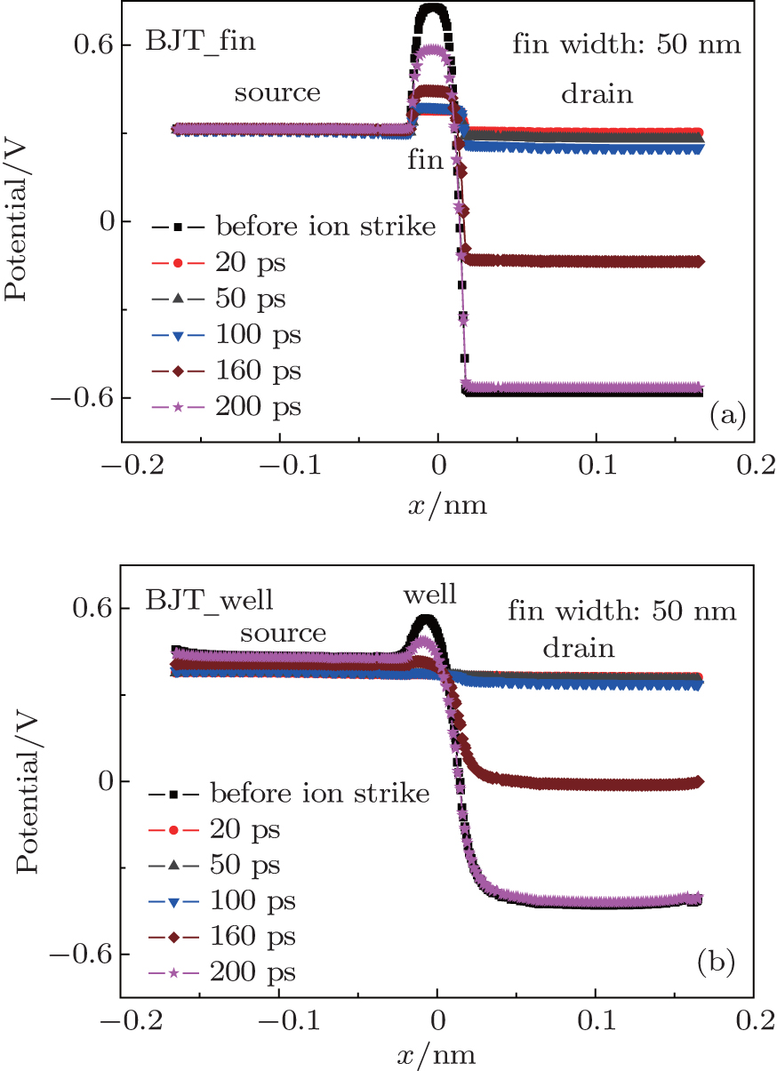 | Fig. 7. Potential profiles in 50-nm fin-width FinFET at different times before and after ion strike. (a) A cut line along the source-fin-drain (x axis). (b) A cut line along the source-well-drain (x axis), which are shown in Fig. 5 as white dot lines, 20 nm above and below the bottom of source/drain region, respectively. The ion LET is 10 MeV· cm2/mg. |
 | Fig. 8. Hole current flowing in 50-nm fin-width FinFET at different times after ion strike. (a) t = 100 ps; (b) t = 200 ps. |
According to the analysis, the base– emitter junction area of BJT_well Ab− e located between the source and the n-well can be calculated as

where LS, WS, and Efin are defined as source length, source width, and fin extension, respectively, in Fig. 1(b). As Wfin increases, the area of BJT_well Ab− e also increases. The injection hole current from source is proportional to this area, namely, [20]

Consequently, FinFETs with wider fin collect more holes and exhibit an increased bipolar amplification and SET pulse width than the narrower devices. This is different from the case of fin-height variations.
The expression of Ab− e is unrelated to Hfin, so the parasitic BJT_well has little variation as the fin height varies. Consequently, with increasing Hfin, the bipolar amplification changes little. However, the charge collection also increases by about 7% as the fin height varies from 35 nm to 55 nm. This is due to the increase in the drain region or the sensitive silicon volume for charge collection in FinFETs. In bulk FinFETs, the drain region dominates the charge collection.[21] Changing Hfin and Wfin can change the drain volume notably. In the simulations, increasing Hfin from 35 nm to 55 nm causes an increase of about 57% of the drain volume, while increasing Wfin brings about only 19% increase. Therefore, increasing fin height can lead to slight increase of charge collection.
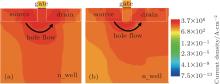
In practice, the drive of a transistor is restricted, so that the effective width of the transistor needs to remain the same in the design. Therefore, the simulation with Wfin/Hfin variations simultaneously is more important. In this case, the effective width of bulk FinFET devices is fixed at 120 nm. Different fin-widths at 10, 20, 30, 40, and 50 nm are employed, and their corresponding fin heights are 55, 50, 45, 40, and 35 nm. As shown in Fig. 9, the charge collection, bipolar amplification, and the SET voltage at FWHM with Wfin/Hfin variations exhibit a similar trend to previous simulation results with different fin-width variations. The charge collection in FinFETs increases about 30% when the Wfin/Hfin varies from 10/55 nm to 50/35 nm, the bipolar amplification increases from 1.27 to 1.61, and the SET voltage at FWHM also increases from 100 ps to 150 ps. This is mainly due to the fact that the combinational effect of Wfin/Hfin variations is dominated by the fin width, while the fin height has a trivial effect on the bipolar amplification and charge collection in bulk p-FinFET.
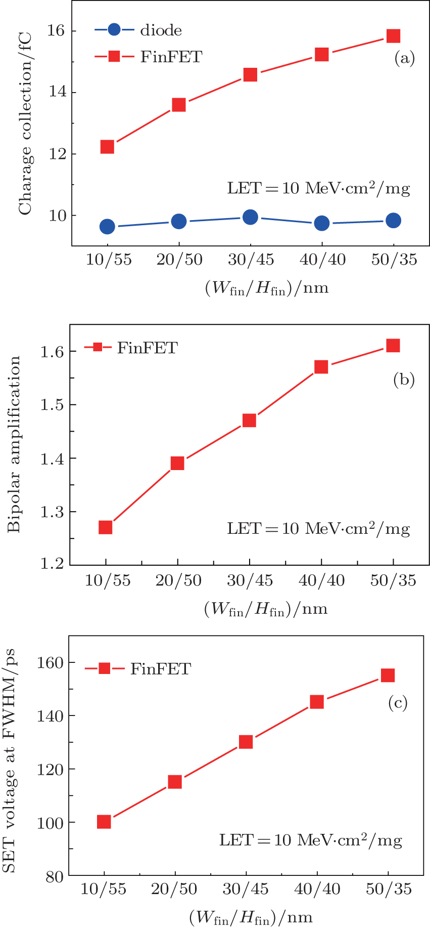 | Fig. 9. (a) Charge collection with different Wfin/Hfin in bulk FinFET versus diode devices. (b), (c) Bipolar amplification and SET voltage at FWHM as a function of Wfin/Hfin in FinFETs, respectively. All simulations are conducted with the same ion LET at 10 MeV· cm2/mg. |
This simulation is meaningful. As shown in Fig. 10, the modulation of Wfin/Hfin can be used to mitigate the generated SET pulse width effectively. Compared with the wider FinFET, the narrow-fin transistor can mitigate the SET pulse width about 35% at least. This improvement results from optimizing the ratio of fin width and height only. The result indicates that reducing the fin width is beneficial for hardening design based on bulk FinFET technology.
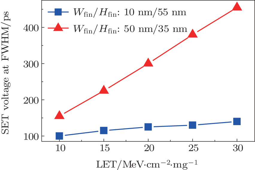 | Fig. 10. Comparison of SET pulse width between two fin-width FinFETs with the same effective width as a function of the ion LETs. |
3D TCAD numerical simulations have been performed to investigate the effect of fin width and height on the bipolar amplification of bulk p-FinFET devices under heavy ion irradiation. Owing to the reduced base– emitter junction area of the BJT_well with decreasing fin width, FinFET with smaller fin width exhibits diminished bipolar amplification and charge collection. The same trend is observed for the fin-width dependence of SET pulse width. However, the fin height shows a trivial effect on bipolar amplification and charge collection in bulk FinFETs. A more practical simulation shows that, the SET pulse width can be mitigated about 35% at least by optimizing the ratio of fin width and height only. This gives a good indication that bulk FinFETs with smaller fin width are more likely to exhibit higher tolerance to SET effect. The results in this work can provide guidance for radiation-hardened bulk FinFET technology and help to design new generations of bulk FinFET transistors with higher tolerance to SEEs.
| 1 |
|
| 2 |
|
| 3 |
|
| 4 |
|
| 5 |
|
| 6 |
|
| 7 |
|
| 8 |
|
| 9 |
|
| 10 |
|
| 11 |
|
| 12 |
|
| 13 |
|
| 14 |
|
| 15 |
|
| 16 |
|
| 17 |
|
| 18 |
|
| 19 |
|
| 20 |
|
| 21 |
|