Chen Long, Payne Justin, Strate Jan, Li Cheng, Zhang Jian-Ming, Yu Wen-Jie, Di Zeng-Feng, Wang Xi. Growth and fabrication of semi-polar InGaN/GaN multi-quantum well light-emitting diodes on microstructured Si (001) substrates. Chinese Physics B, 24(11): 118102
Permissions
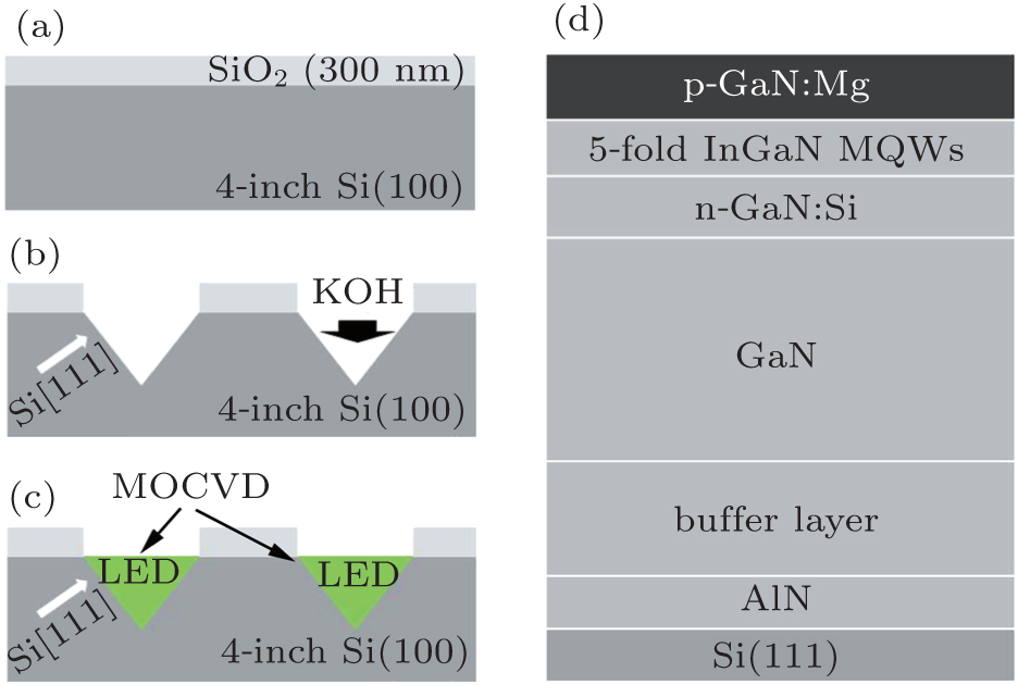
Growth and fabrication of semi-polar InGaN/GaN multi-quantum well light-emitting diodes on microstructured Si (001) substrates
Chen Longa),b), Payne Justinb), Strate Janb), Li Chengb), Zhang Jian-Mingb), Yu Wen-Jiea), Di Zeng-Fenga), Wang Xia)
State Key Laboratory of Functional Materials for Informatics, Institute of Microsystem and Information Technology, Chinese Academy of Sciences, Shanghai 200050, China
Shanghai Simæra Incorporated, Shanghai 201800, China
Semi-polar (1 − 101) InGaN/GaN light-emitting diodes were prepared on standard electronic-grade Si (100) substrates. Micro-stripes of GaN and InGaN/GaN quantum wells on semi-polar facets were grown on intersecting {111} planes of microscale V-grooved Si in metal–organic vapor phase epitaxy, covering over 50% of the wafer surface area. In-situ optical reflectivity and curvature measurements demonstrate that the effect of the thermal expansion coefficient mismatch was greatly reduced. A cross-sectional analysis reveals low threading dislocation density on the top of most surfaces. On such prepared (1 − 101) GaN, an InGaN/GaN LED was fabricated. Electroluminescence over 5 mA to 60 mA is found with a much lower blue-shift than that on the c-plane device. Such structures therefore could allow higher efficiency light emitters with a weak quantum confined Stark effect throughout the visible spectrum.
GaN-based devices have been used widely for optical and electronic applications. Nowadays, most of these devices such as the light emitting diode (LED) are fabricated on GaN template sapphire and silicon carbon in the commercial sector. In spite of some difficulties involved, ongoing research focuses more and more on the growth of GaN-based devices on Si substrates to reduce costs. In addition, the potential of integrating conventional Si integrated circuits with GaN based devices on a single wafer is also an attractive prospect, which will open the possibility for opto-electronics integration. The GaN/Si platform will enable monolithic integration of III– V compound semiconductor electronic and opto-electronic components along with traditional Si CMOS circuit elements on a single microchip, [1] such as a high-density information processor, precision image sensor, and/or display. If we could fabricate a laser diode (LD) on a silicon substrate, it might be integrated with a driver/signal processing circuits to offer a new possibility in silicon photonics.
However, the growth technique on Si substrates is quite challenging. In order to achieve high-quality crack-free epitaxial layers, the high lattice mismatch and large differences in thermal expansion coefficients need to be taken into account and be compensated.[2] The major methodology for the growth of III– V on Si substrates is to control the stress in the layer stack, monitored by in-situ measurements of the curvature of the wafer during epitaxy. Different approaches of strain engineering can be found in the literature in order to achieve a crack-free layer after cool down. Most of them use multiple-intermediate layers.[3– 6] Another way is reducing the size of the crystal on the substrate.[7]
In spite of the rapid developments in the high-brightness LEDs, the efficiency of an LED, especially in the green light region, still needs to be improved. One of the main issues is believed to be the strong spontaneous polarization field induced at the hetero-interface on polar (0001) GaN.[8] To decrease the detrimental influence of the polarization field, quantum wells grown on semi-polar GaN, such as {1 − 101} GaN and {11-20} GaN, have been attempted.[9– 11] However, to achieve a practically acceptable device, the improvement of growth conditions is still to be studied.
In this work, a selective area growth (SAG) of GaN on a patterned silicon substrate is proposed. By providing Si {111} facets in patterned Si (100) substrates, we are now able to get a semi-polar {1 − 101} GaN template on a 4” silicon wafer via epitaxial lateral overgrowth (ELO). It is shown that c-plane AlN/AlGaN/GaN buffer layers semi-polar plane InGaN/GaN MQW can be grown selectively on these Si {111} facets. This approach also reduces the required effort for strain engineering during epitaxy due to the reduced thermal expansion mismatch through the separated growth area and the tilt of crystal axis. By using two equivalent Si {111} facets in trenches, tilted by 54.7 degree, the active emission area can be increased theoretically by a factor of 1.7 in comparison to the planer area.
2. Experimental details
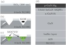
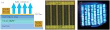
To prepare the growth substrate, 525-μ m-thick 4-inch n-doped Si (100) wafers were used for lithography. An anisotropic wet etch (KOH) is applied on masked wafers to create trenches, as shown in Fig. 1. Trenches measured a period of 8 μ m with a top width opening of ∼ 3.5 μ m, and a top length opening of 90 μ m with a spacing of 10 μ m, respectively. A 300-nm-thick silicon oxide layer was grown by low pressure chemical vapor deposition (LPCVD) as the mask layer (Fig. 1(a)). The facing pairs of Si {111} facets are naturally exposed because of an anisotropic etch rate in the [100] and [111] directions (Fig.1(b)). Using MOCVD, all heterostructures were grown on the Si {111} facets (Fig. 1(c)). This step was performed in an AIXTRON G5 14 × 4” reactor and the growth procedure was given as follows. First, the substrate was heated to 1110 ° C in H2 ambient for a 10-min thermal cleaning. Next, a 10-nm AlN nucleation layer and 100-nm high-temperature AlN buffer layer were grown at 1070 ° C and 1170 ° C, respectively. Then, a 250-nm AlGaN buffer layer was deposited with decreasing Al content.
Fig. 1. (a) 4-inch Si (100) wafer with SiO2 mask. (b) Trenches are developed by KOH. (c) MOCVD growth on Si (111) facets. (d) LED layer stack used on Si(111) substrate and patterned Si (100) substrate.
Two different sample structures are reported: GaN and a full MQW LED structure. The GaN structure was grown without doping to a thickness of several micros, characterized in-situ. A separate full LED structure was grown on 500-nm Si-doped GaN, a 5-period InGaN/GaN QW stack, and a 150-nm Mg-doped GaN layer, shown in Fig. 1(d). Standard electronic-grade 625-μ m Si (111) planer substrates were put into the chamber for comparison. Trimethyl gallium (TMGa), trimethyl indium (TMIn), and trimethyl aluminum (TMAl) were used as group-III sources and ammonia (NH3) as the group V source. Silane (SiH4) and biscyclopentadienyl magnesium (Cp2Mg) were used as dopants. Hydrogen (H2) was used as the carrier gas, except for MQW growth, in which nitrogen (N2) was employed.
Full spectroscopic measurements of reflectivity and curvature at different wavelengths between 450 nm and 950 nm by a measurement tool from LayTec with additional true-temperature pyrometer module enables monitoring and controlling the growth surface temperature, film formation and wafer bending during epitaxy. Growth morphology was assessed by scanning electron microscopy (SEM). Scanning (STEM) and transmission electron microscopy (TEM) micrographs were prepared for analysis of the micro-stripe cross sections. Optoelectronic properties are determined by electroluminescence measurements (EL). For functional testing, lateral LED devices were fabricated. A semi-transparent 8-nm Ni/8-nm Au p-contact was deposited by electron-beam evaporation and defined by photolithography and lift-off. Ti/Al/Ti/Au was employed, constituting the n-contact as well as the probing pad.
3. Results and discussion
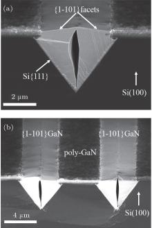
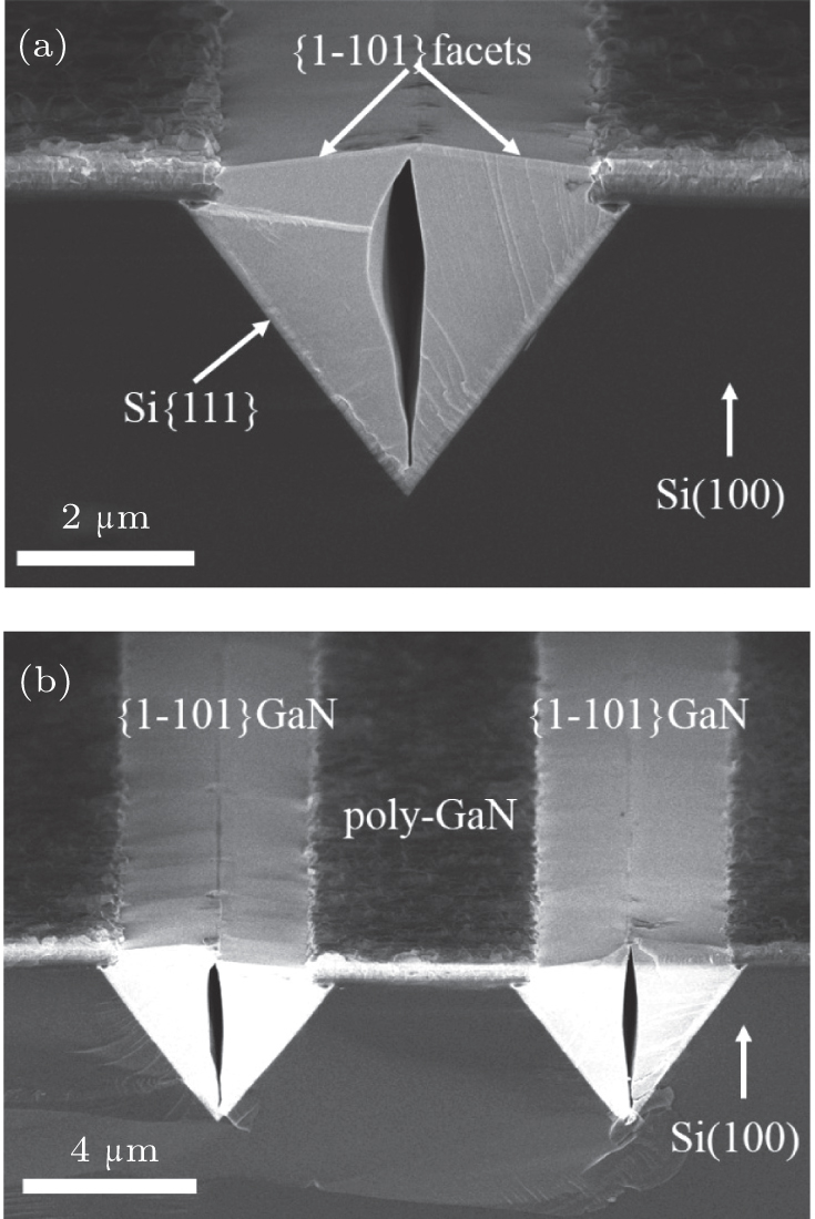
Figure 2(a) shows the cross-sectional scanning electron microscopy (SEM) image of the samples with GaN growth. GaN grows along its (0001) axis on the opposite {111} Si side walls initially and at the same time develops the {1 − 101} GaN facets toward the surface. After 50 minutes, the two opposite GaN layers collide and coalesce with each other in the trenches and the two opposite {1 − 101} GaN facets are well developed with a flat surface morphology as depicted in Fig. 2(b). These two {1 − 101} GaN facets form a new growth plane for deposition in the next step. On SiO2, parasitic poly-crystalline GaN are formed at the same time due to the initially deposited AlN nucleation layer, which can be explained by the lack of growth selectivity of the Al-containing layer over commonly used dielectric masks and substrates.[12, 13]
Fig. 2. (a) Cross-sectional SEM and (b) the bird-view SEM images of GaN on V-grooved Si (100) substrate, respectively.
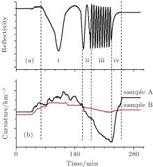
The in-situ reflectance (Fig. 3(a)) reveals steps of epitaxy, such as the growth of AlN (i), AlGaN (ii), and GaN (iii), as well as cooling down (iv). As reported previously, wafer bowing and cracks often appear in the growth of GaN on Si as a result of the tensile strain induced by their large mismatch in thermal expansion coefficients (56%). However, in this study, at the end of cooling down, the patterned Si (100) substrate has a much lower curvature than the Si (111) as shown in Fig. 3(b). Patterned Si (100) substrates experienced less curvature variation than planer Si (111) substrates. The tensile strain inside is believed to be almost equal to those found in the strain free sample. It is likely due to the reduced thermal expansion mismatch through reducing the size of the crystal on the substrate, [14, 15] and the tilt of the crystal axis.[16] Sawaki et al. have calculated that the strain ε 〈 1− 100〉 and ε 〈 0001〉 normal to the stripe is much lower than that ε 〈 11− 20〉 along the stripe direction.[17] Therefore, in this work, the trenches along the (110) and (1 − 10) directions on Si (100) are both developed equally in quantity and distribution to balance the strain generated in both directions and reduce the wafer bowing.
Fig. 3. Traces of in-situ measurements for the whole growth process of GaN epilayer. (a) Optical reflectivity on 4-inch Si (111). (b) Wafer curvature on different substrates: sample A, Si (111) and sample B, Si (100).
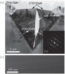
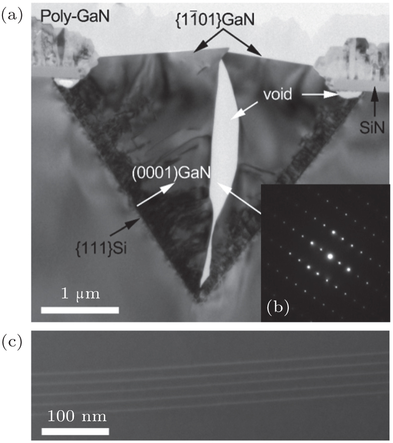
An analysis of the stripe cross section in TEM and STEM is summarized in Fig. 4. Figure 4(a) shows a cross-sectional bright-field TEM image of an InGaN/GaN MQW sample taken as the electron beam which is incident along the 〈 11 − 20〉 direction. The misfit dislocations created at the AlGaN/AlN/Si hetero-interface propagate along the growth direction of 〈 0001〉 . However, during the growth until the coalescence, some of them turn to the direction perpendicular to the growth axis and others end at the surface inside the trench. It is worth mentioning that the SiO2 overhang of about 0.3 μ m originates from the wet-etching step. Under the overhang, several dislocations along the direction normal to the growth axis are suppressed successfully. Thus, the density of threading dislocation can be decreased drastically on the {1 − 101} GaN facets. To determine the residual stress in the {1 − 101} GaN, we perform selective area electron diffraction (SAED) so as to deduce a value of lattice constant c of 0.5191 nm based on the spacing between the diffraction spots in the SAED patterns. This value is very close to the value of 0.5185 nm, which is obtained on a strain free GaN, indicating that the residual stress is effectively reduced via reducing the size of the crystal on the substrate and the tilt of the crystal axis. The cross-sectional STEM image (Fig. 4(c)) shows the InGaN/GaN MQW on the {1 − 101} GaN facet with a higher magnification, which reveals that there is likely no threading dislocation observed in this region. Abrupt and flat interfaces between the MQW layers can be clearly seen.
Fig. 4. Cross-sectional analysis of the GaN-based microstripes in the Si grooves. (a) Bright-field TEM image of the entire stripe revealing dislocations and interface. (b) Selective area electron diffraction pattern (SAED) of the GaN area. (c) STEM of the QW portion.
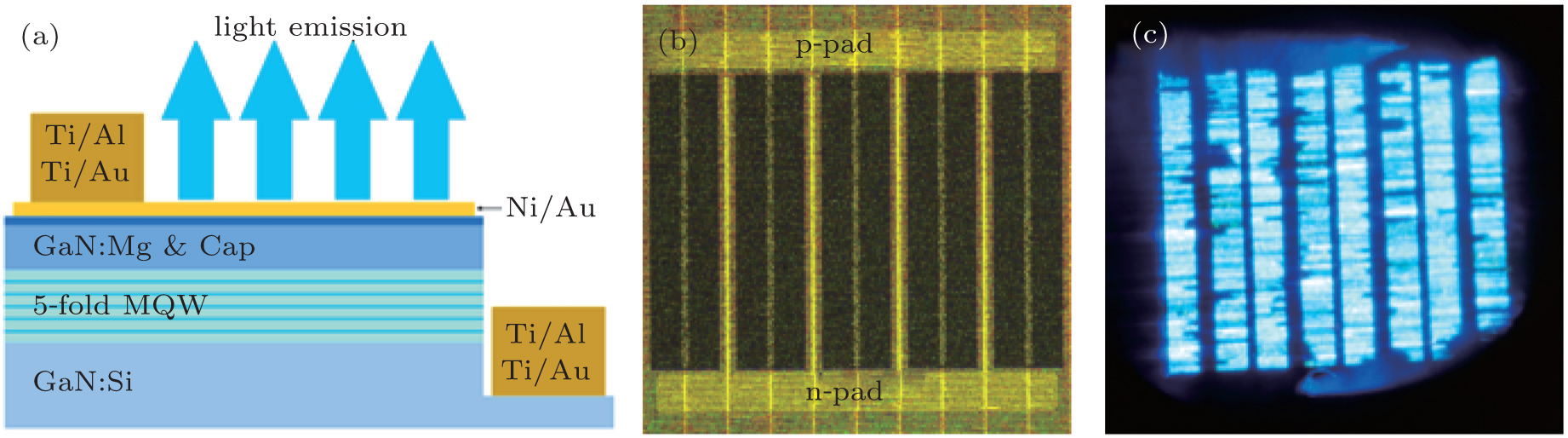
The full micro-stripe LED structure was analyzed under electrical injection. Figure 5(a) shows the schematic structure of a (1 − 101) GaN microstripe LED. One end of the GaN stripes was etched down to the Si-doped layer for the n contact. We successfully achieved an array of uniform (1 − 101) GaN microstripe LEDs, which are parallel connected, as shown in Fig. 5(b). Bright blue electroluminescence (EL) (Fig. 5(c)) was observed at the base of the Ni/Au p-contact with annealing under air atmosphere at 495 ° for 10 min. However, not every area along the stripe direction emits light for quite a few {1 − 101} GaN microstripe LEDs, which is likely due to the series resistance in the ultrathin Ni/Au film and/or limited lateral transport in the GaN layer. A more sophisticated device structure and process conditions have to be established and is in process.
Fig. 5. (a) Schematic structure of a (1 − 101) GaN microstripe LED. (b) An optical microscopic image of the InGaN/GaN MQW LED devices. (c) Photos showing electroluminescence of LED taken though the optical microscope.
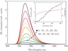
Typical LED performance is demonstrated in Fig. 6. The emission spectra (Fig. 6) are shown as a function of the driving current. We find that the peak wavelength is blue shifted by 6 nm under variation of current density over a factor of ten. This is much less than the values of 20 nm reported for samples made on (001) sapphire substrate. The current-voltage measurement shows the turn-on voltage around 3 V (Fig. 6, inset). At 3.8 V, a current of 60 mA is measured. There is a slight leakage under reverse polarity, which can be improved by the utilization of appropriate processing techniques used in the industry. EL was collected with a 3” integrating sphere and a CCD spectrometer. The calibration of the system allows for a measurement of the total light output power of the LED. The collected power increases with current (3 mA to 60 mA) and reaches 1.83 mW corresponding to an external quantum efficiency (EQE) of 0.8%. This low value is likely the result of the highly absorptive Si surroundings and the block by the semitransparent Ni/Au film, which should improve in future steps of substrate removal and device structure optimization.
Fig. 6. Electroluminescence spectra of semi-polar InGaN/GaN microstripe LED at various drive current levels. Spectra are dominated by a peak at 475 nm that does not shift so much when current increases fivefold. The insert show the I– V characteristics and the light output power.
4. Conclusions
In summary, the growth of semipolar {1 − 101} GaN and {1 − 101} InGaN/GaN MQWs on 4” V-grooved (001) Si substrates were demonstrated. Microstripe LEDs were successfully fabricated. The thermal expansion mismatch was significantly reduced compared to the planer Si (111) substrate. Wavelength-stable EL emission was achieved with a dominant wavelength of 475 nm at a collected power of 1.83 mW. The semi-polar LED showed a weak blue shift as a function of the driving current, suggesting a weak quantum confined Stark effect. This approach is promising for producing high-performance {1 − 101} GaN-based optical devices on (001) Si for Si phonics.
ChenG T, ChangS P, ChyiJ I and ChangM N2008Appl. Phys. Lett. 92241904DOI:10.1063/1.2946655[Cited within:1]
10
XuS R, HaoY, ZhangJ C, XueX Y, LinZ Y, LiuZ Y, MaJ C, LüL, LiP X, HeQ and LiJ T2011Chin. Phys. B20107802DOI:10.1088/1674-1056/20/10/107802[Cited within:1]
11
HuQ, WeiT B, DuanR F, YangJ K, HuoZ Q, LuT C and ZengY P2009Chin. Phys. Lett. 26096801DOI:10.1088/0256-307X/26/9/096801[Cited within:1]
... V compound semiconductor electronic and opto-electronic components along with traditional Si CMOS circuit elements on a single microchip,[1] such as a high-density information processor, precision image sensor, and/or display ...
1
2004
0.0
0.0
... [2] The major methodology for the growth of III#cod#x2013 ...
1
2002
0.0
0.0
... [3#cod#x2013 ...
1
2013
0.0
0.0
1
2003
0.0
0.0
1
2014
0.0
0.0
... 6] Another way is reducing the size of the crystal on the substrate ...
1
2002
0.0
0.0
... [7] ...
1
1997
0.0
0.0
... [8] To decrease the detrimental influence of the polarization field, quantum wells grown on semi-polar GaN, such as {1 #cod#x2212 ...
1
2008
0.0
0.0
... [9#cod#x2013 ...
1
2011
0.0
0.0
1
2009
0.0
0.0
... 11] However, to achieve a practically acceptable device, the improvement of growth conditions is still to be studied ...
1
1998
0.0
0.0
... [12,13] ...
1
2008
0.0
0.0
... [12,13] ...
1
2002
0.0
0.0
... It is likely due to the reduced thermal expansion mismatch through reducing the size of the crystal on the substrate,[14,15] and the tilt of the crystal axis ...
1
2001
0.0
0.0
... It is likely due to the reduced thermal expansion mismatch through reducing the size of the crystal on the substrate,[14,15] and the tilt of the crystal axis ...
1
2002
0.0
0.0
... [16] Sawaki et al ...
1
2011
0.0
0.0
... [17] Therefore, in this work, the trenches along the (110) and (1 #cod#x2212 ...
Growth and fabrication of semi-polar InGaN/GaN multi-quantum well light-emitting diodes on microstructured Si (001) substrates
[Chen Longa),b), Payne Justinb), Strate Janb), Li Chengb), Zhang Jian-Mingb), Yu Wen-Jiea), Di Zeng-Fenga), Wang Xia)]


 , Payne Justin