Chen Wei-Jie, Han Xiao-Biao, Lin Jia-Li, Hu Guo-Heng, Liu Ming-Gang, Yang Yi-Bin, Chen Jie, Wu Zhi-Sheng, Liu Yang, Zhang Bai-Jun. Migration characterization of Ga and In adatoms on dielectric surface in selective MOVPE* . Chinese Physics B, 24(11): 118101
Permissions
Migration characterization of Ga and In adatoms on dielectric surface in selective MOVPE*
Chen Wei-Jiea),b), Han Xiao-Biaoa),b), Lin Jia-Lia),b), Hu Guo-Henga),b), Liu Ming-Ganga),b), Yang Yi-Bina),b), Chen Jiea),b), Wu Zhi-Shenga),b), Liu Yangb), Zhang Bai-Juna),b)
State Key Laboratory of Optoelectronic Materials and Technologies, Sun Yat-Sen University, Guangzhou 510275, China
School of Physics and Engineering, Institute of Power Electronics and Control Technology, Sun Yat-Sen University, Guangzhou 510275, China
*Project supported by the National Natural Science Foundation of China (Grant Nos. 61274039 and 51177175), the National Basic Research Program of China (Grant No. 2011CB301903), the Ph.D. Programs Foundation of Ministry of Education of China (Grant No. 20110171110021), the International Sci. & Tech. Collaboration Program of China (Grant No. 2012DFG52260), the International Sci. & Tech. Collaboration Program of Guangdong Province, China (Grant No. 2013B051000041), the Science and Technology Plan of Guangdong Province, China (Grant No. 2013B010401013), the National High Technology Research and Development Program of China (Grant No. 2014AA032606), and the Opened Fund of the State Key Laboratory on Integrated Optoelectronics, China (Grant No. IOSKL2014KF17).
Abstract
Migration characterizations of Ga and In adatoms on the dielectric surface in selective metal organic vapor phase epitaxy (MOVPE) were investigated. In the typical MOVPE environment, the selectivity of growth is preserved for GaN, and the growth rate of GaN micro-pyramids is sensitive to the period of the patterned SiO2 mask. A surface migration induced model was adopted to figure out the effective migration length of Ga adatoms on the dielectric surface. Different from the growth of GaN, the selective area growth of InGaN on the patterned template would induce the deposition of InGaN polycrystalline particles on the patterned SiO2 mask with a long period. It was demonstrated with a scanning electron microscope and energy dispersive spectroscopy that the In adatoms exhibit a shorter migration length on the dielectric surface.
Keyword:
81.05.Ea; 81.15.Gh; 81.16.Rf; 47.57.ef; metal organic vapor phase epitaxy; selective area growth; migration length
GaN and its related III– N compounds have attracted a great deal of attention for their applications in optical devices.[1– 8] Compared with the conventional III– N devices on c-plane GaN, the superior properties of light emitting diodes (LEDs) grown on three-dimensional GaN micro-structures by selective metal organic vapor phase epitaxy (MOVPE) have been demonstrated.[9– 13] The hexagonal GaN micro-pyramid is one kind of the most promising building blocks for the high-performance optoelectronic devices because there is a possibility to reduce the threading dislocations[14] and suppress the undesirable spontaneous and piezoelectric polarization fields.[15, 16] Highly efficient LEDs grown on GaN micro-pyramids have been successfully realized by selective area growth (SAG) technology in the MOVPE system.[17– 19] In order to realize the potential of LEDs on GaN micro-pyramids, the precise control of the morphology of the GaN micro-pyramid and the alloy component of the InGaN active layer on the GaN micro-pyramid is pressingly needed. The influence of the reactor temperature, pressure, and growth time on the formation of the GaN micro-pyramids have been reported previously.[20– 24] Another key factor affecting the selective area growth of III– N materials on the patterned template in the MOVPE system is the migration behavior of the chemical species on the dielectric surface. Specifically, the growth rate of the GaN micro-pyramids and the In-incorporation efficiency of the InGaN active layers are sensitive to the migration characterizations of Ga and In adatoms. However, little research related to the surface migration of Ga and In adatoms on the dielectric surface during SAG has been reported.
In this work, we report on the migration characterizations of Ga and In adatoms on the dielectric surface. After the re-growth of GaN micro-pyramids and pyramidal micro-LEDs embedded with InGaN active layers (μ -LEDs), the surface morphology of the patterned SiO2 mask with different periods is investigated. In the typical MOVPE growth environment for InGaN-based blue LEDs, the effective migration length of Ga and In adatoms on the patterned SiO2 mask is studied.
2. Experiment
The growth experiments were carried out in a low-pressure MOVPE system. The patterned SiO2/AlN/Si templates used for selective area growth were prepared as follows. The 2-inch Si (111) substrates were etched in an HF:H2O solution, rinsed in deionized water, and dried immediately before loading into the MOVPE chamber. A 50 nm-thick AlN film was grown on the Si substrate at 1095 ° C, which served as a seeding layer for subsequent re-growth. Before re-growth in MOVPE, a 100 nm-thick SiO2 layer was deposited on the AlN/Si template via plasma enhanced chemical vapor deposition (PECVD) as a mask. Subsequently, circle openings with different periods were fabricated on the SiO2 layer by standard lithographic procedures and chemical wet etching. After chemical cleaning, the patterned SiO2/AlN/Si templates were reloaded into the MOVPE chamber. The reactor temperatures for the growth of the GaN micro-pyramid structure and the InGaN active layers were 1095 ° C and 800 ° C, which are typical growth parameters for the epitaxy of InGaN-based blue LEDs. TMGa, TMAl, TMIn, and NH3 were used as the source materials for Ga, Al, In, and N, respectively. GaN micro-pyramids and pyramidal micro-LEDs embedded with InGaN active layers grown on the patterned templates with different periods were prepared to investigate the migration behaviors of Ga and In adatoms on the dielectric surface, respectively. The InGaN-based pyramidal micro-LED consisted of an n-GaN micro-pyramid base, three pairs of InGaN/GaN multiple quantum wells (MQWs), and a p-GaN cap layer. The morphologies of all samples were characterized by a scanning electron microscope (SEM) with an acceleration voltage of 5 kV. The particular elements of the materials deposited on the patterned SiO2 mask were analyzed by energy dispersive spectroscopy (EDS).
3. Results and discussion
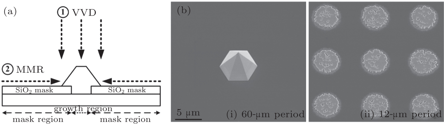
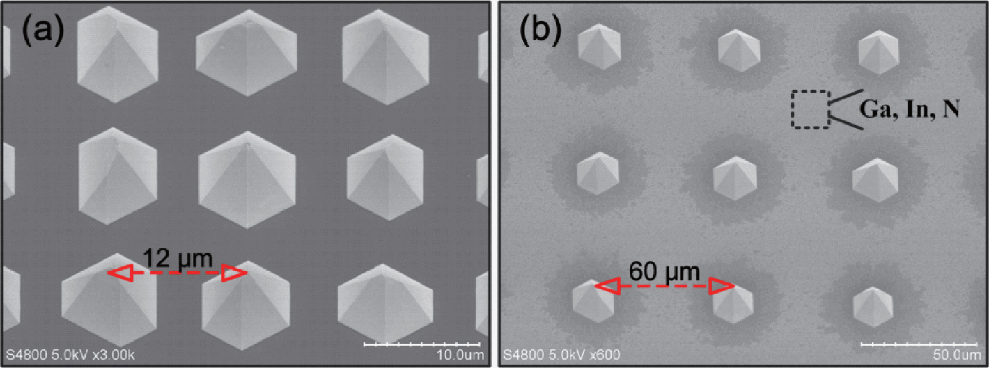
In selective MOVPE, there are two main source supply paths, [25, 26] as illustrated in Fig. 1(a). The first one is the vertical vapor-phase diffusion (VVD) by which the source materials directly reach the substrate from the ceiling. The other one is the surface migration from the mask region (MMR) by which the source materials migrate from the dielectric mask region to the growth region. For III– N materials selectively grown on patterned templates, the major factor affecting the growth rate of the III– N materials is the source supply from the MMR. Figure 1(b) shows the SEM images of GaN selectively grown on patterned SiO2/AlN/Si templates with different periods for 5 min. Both patterned SiO2 masks are periodic circle-openings of 5 μ m in diameter. The period of the circle-openings is 60 μ m for sample (i) and 12 μ m for sample (ii). After re-growth, a well-shaped GaN micro-pyramid with mirror-like side facets is found on the 60-μ m-period patterned template, while sample (ii) on the 12-μ m-period patterned template has a membranous structure with jagged sidewalls and some inversed-pyramid vacancies. Each GaN micro-structure’ s size of sample (i) is much larger than that of sample (ii), indicating the increased growth rate of GaN on the patterned template with a longer period. Furthermore, there are no precipitates deposited on the SiO2 mask regions of both samples, demonstrating that the selectivity of growth is preserved for GaN during SAG in MOVPE.[27] Therefore, the Ga source materials could migrate effectively from the mask region to the growth region without deposition on the dielectric mask, leading to the enhancement of the Ga source supply from the MMR and an accompanying increased growth rate.
Fig. 1. (a) Diagram of the source supply paths in selective MOVPE. (b) SEM images of GaN selectively grown on patterned templates with different periods. The patterned mask’ s period of sample (i) is 60 μ m and that of sample (ii) is 12 μ m.
As demonstrated above, the growth rate of GaN on the patterned template increased as the patterned mask’ s period became longer. However, once the period became longer than twice the migration length of Ga adatoms on the dielectric mask, the additional Ga source supply from the MMR was unable to reach the growth region from the mask region and increase the growth of GaN anymore. In order to figure out the effective migration length of Ga adatoms on the dielectric surface, a special patterned SiO2/AlN/Si template was adopted. The configuration of the special patterned template is illustrated in Fig. 2(a). Half of the template is fully covered by SiO2 film without any patterns, while the other half is patterned by circle-openings of 3 μ m in diameter and 12 μ m in period. Due to the great selectivity of GaN on the dielectric surface, the Ga source materials that reached the mask fully covered by SiO2 could migrate to the patterned regions along the SiO2 surface. Once the Ga source materials reached the growth region in the patterned region, they deposited on the exposed AlN surface and formed GaN in the N-rich MOVPE environment. Because of the limited migration length of Ga adatoms on the dielectric surface, the quantity of Ga source materials that could arrive to the growth region decreased as the distance away from the boundary between two regions increased. Therefore, the size of the GaN micro-pyramid on the patterned region would decrease along with the increasing distance, which reflects the migration behavior of Ga adatoms on the dielectric surface. The variation of the GaN micro-pyramids’ morphology along with the increasing distance is shown in Fig. 2(b). Near the boundary, a pyramid with a nano-sized tip and a diameter of about 10 μ m is observed. With increasing distance, the size of the pyramid becomes smaller and the pyramid structure turns into a truncated pyramid structure with a larger top surface. When the distance is larger than 300 μ m, no obvious change of the pyramid is found. It means that the growth of the GaN micro-pyramids at the distance larger than 300 μ m is not affected by the migration of Ga adatoms from the mask region fully covered by the SiO2 layer anymore.
Fig. 2. (a) Illustration of the specific patterned mask. (b) The variation of GaN micro-pyramids’ morphology along with increasing distance away from the boundary.
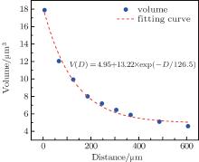
Statistical analysis on the size of the GaN micro-pyramids was performed. The volumes of the micro-pyramids are plotted as a function of the distance in Fig. 3. Firstly, a significant decrease in the volume is observed. As the distance increases further, the declining rate becomes slow. An exponential decrease trend is observed. The relation between the volume of the pyramid and the distance is fitted with the following equation:
where V(D) is the volume of the GaN micro-pyramid at the distance D away from the boundary, V0 describes the GaN micro-pyramid’ s volume at the distance which is much larger than the migration length of Ga adatoms, C is an attenuation coefficient, and L is the effective migration length of Ga adatoms on the dielectric surface. The values of V0, C, and L are related to the MOVPE growth parameters, such as the growth temperature, the pressure of the reactor, the ratio of V/III, etc. In this work, we just figure out the migration length of Ga adatoms on the dielectric surface in the typical MOVPE growth environment. Further researches about the relation between the migration length of Ga adatoms and the MOVPE growth parameters will be discussed in other works. A good fit of the data (red dotted line) is obtained. The fitted migration length of Ga adatoms on the dielectric surface of about 120 μ m is evaluated. The value of each parameter in Eq. (1) is given in Fig. 3 as well. Accordingly, in order to achieve effective migration of Ga adatoms from the mask region to the growth region, the period of the patterned mask should be smaller than twice the migration length of Ga adatoms, because the Ga source materials that arrive at the SiO2 mask migrate to both sides of the mask.
Fig. 3. Variation of the micro-pyramids’ volume versus the distance away from the boundary.
Figure 4 shows the SEM images of pyramidal micro-LEDs embedded with InGaN active layers grown on 12-μ m-period and 60-μ m-period patterned templates. No precipitates are observed on the 12-μ m-period patterned SiO2 mask, while there are some polycrystalline particles without specific crystallographic orientations deposited on the 60-μ m-period patterned SiO2 mask. An energy dispersive spectroscopy measurement was performed to identify the particular elements of the polycrystalline particles. It is found that the precipitates consist of Ga, In, and N elements. As demonstrated, the selectivity of the growth is preserved for all GaN layers during SAG in MOVPE. Thus, the polycrystalline particles on the SiO2 mask are believed to form during the growth of the InGaN active layers, indicating that the In adatoms exhibit weaker migration ability on the dielectric surface.
Fig. 4. SEM images of μ -LEDs grown on (a) 12-μ m-period and (b) 60-μ m-period patterned templates.
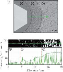
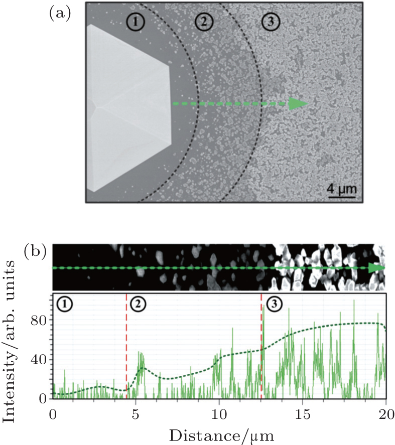
A high magnification SEM image of a μ -LED grown on 60-μ m-period patterned template and its surrounding SiO2 mask is shown in Fig. 5(a), which is used to reveal the migration behavior of the In adatoms on the dielectric surface. Around the μ -LED, a region ① nearly free of polycrystalline particles is observed, which is about 4– 5 μ m away from the μ -LED. As the distance increases, some sparse InGaN polycrystalline particles deposit on the region ② , which is a transitional zone for the In adatoms that have migrated from the mask region to the growth region. A mass of InGaN polycrystalline particles are found on the mask of region ③ , indicating the deposition of polycrystalline particles on the dielectric mask during the migration of Ga adatoms from the mask region to the growth region. The EDS line analysis of the Ga Kα emission was utilized to determine the quantity of precipitates on the SiO2 mask, as shown in Fig. 5(b). Gallium is hardly detected in region ① . However, the intensity of the Ga Kα emission enhances along with the increase of the distance away from the μ -LED, indicating more InGaN polycrystalline particles depositing on the SiO2 mask far away from the growth region. The EDS measurement is in good agreement with the SEM result. Accordingly, the migration length of In adatoms on the dielectric surface is estimated to be about 4– 5 μ m. Compared with Ga adatoms, the In adatoms have a shorter migration length on the dielectric surface, which is attributed to the lower growth temperature of InGaN and the heavier mass of the In atom. For the μ -LED grown on the 12-μ m-period patterned template, the distance between two micro-pyramids after the growth of the n-GaN micro-pyramid base is less than 8 μ m. Therefore, the In adatoms could migrate to the growth region before deposition on the SiO2 mask during the growth of the InGaN active layers. However, the distance between two μ -LEDs grown on the 60-μ m-period patterned template is larger than 40 μ m, which is too long for the In adatoms to migrate from the mask region to the growth region. Thus, the In adatoms deposit on the SiO2 mask. Although the effective migration length of Ga adatoms on the dielectric surface is larger than 40 μ m, the Ga adatoms would be adsorbed by the In adatoms once the In adatoms deposit on the mask. As a result, InGaN polycrystalline particles form on the SiO2 mask during the growth of the InGaN active layers.
Fig. 5. (a) A high magnification SEM image of a μ -LED grown on 60-μ m-period patterned template and its surrounding SiO2 mask. (b) EDS line analysis of the Ga Kα emission from region ① to region ③ .
4. Conclusion
We reported the migration characterizations of Ga and In adatoms on the dielectric surface during selective MOVPE. The growth rate of GaN on the patterned template with a longer period was increased as a result of the additional Ga source supply from MMR. In the typical MOVPE environment, the migration length of Ga adatoms on the dielectric surface has been figured out. It was observed that the selectivity of growth was preserved for GaN, while InGaN polycrystalline particles were found to deposit on the 60-μ m-period patterned mask after the growth of μ -LEDs. It was demonstrated with scanning electron microscope and energy dispersive spectroscopy that the In adatoms exhibit a shorter migration length on the dielectric surface.
... 8] Compared with the conventional III#cod#x2013 ...
1
1997
0.0
0.0
... [9#cod#x2013 ...
1
2006
0.0
0.0
1
2007
0.0
0.0
1
2014
0.0
0.0
1
2014
0.0
0.0
... 13] The hexagonal GaN micro-pyramid is one kind of the most promising building blocks for the high-performance optoelectronic devices because there is a possibility to reduce the threading dislocations[14] and suppress the undesirable spontaneous and piezoelectric polarization fields ...
1
1999
0.0
0.0
... 13] The hexagonal GaN micro-pyramid is one kind of the most promising building blocks for the high-performance optoelectronic devices because there is a possibility to reduce the threading dislocations[14] and suppress the undesirable spontaneous and piezoelectric polarization fields ...
1
1998
0.0
0.0
... [15,16] Highly efficient LEDs grown on GaN micro-pyramids have been successfully realized by selective area growth (SAG) technology in the MOVPE system ...
1
2012
0.0
0.0
... [15,16] Highly efficient LEDs grown on GaN micro-pyramids have been successfully realized by selective area growth (SAG) technology in the MOVPE system ...
1
2005
0.0
0.0
... [17#cod#x2013 ...
1
2007
0.0
0.0
1
2011
0.0
0.0
... 19] In order to realize the potential of LEDs on GaN micro-pyramids, the precise control of the morphology of the GaN micro-pyramid and the alloy component of the InGaN active layer on the GaN micro-pyramid is pressingly needed ...
1
1998
0.0
0.0
... [20#cod#x2013 ...
1
1999
0.0
0.0
1
2000
0.0
0.0
1
2014
0.0
0.0
1
2014
0.0
0.0
... 24] Another key factor affecting the selective area growth of III#cod#x2013 ...
1
1993
0.0
0.0
... Results and discussionIn selective MOVPE, there are two main source supply paths,[25,26] as illustrated in Fig ...
1
2000
0.0
0.0
... Results and discussionIn selective MOVPE, there are two main source supply paths,[25,26] as illustrated in Fig ...
1
1998
0.0
0.0
... [27] Therefore, the Ga source materials could migrate effectively from the mask region to the growth region without deposition on the dielectric mask, leading to the enhancement of the Ga source supply from the MMR and an accompanying increased growth rate ...
Migration characterization of Ga and In adatoms on dielectric surface in selective MOVPE*
[Chen Wei-Jiea),b), Han Xiao-Biaoa),b), Lin Jia-Lia),b), Hu Guo-Henga),b), Liu Ming-Ganga),b), Yang Yi-Bina),b), Chen Jiea),b), Wu Zhi-Shenga),b), Liu Yangb), Zhang Bai-Juna),b)]


 , Zhang Bai-Jun