


[Peng Ruia), b) , Xu Hai-Chaoa), b)  , Feng Dong-Lai
a), b) ]
, Feng Dong-Lai|
|


†Corresponding author. E-mail: xuhaichao@fudan.edu.cn
*Project supported by the National Natural Science Foundation of China and the National Basic Research Program of China (Grant Nos. 2012CB921402, 2011CB921802, and 2011CBA00112).
The discovery of high temperature superconductivity in single-layer FeSe/SrTiO3 provides a new platform for exploring superconductivity and pursuing higher Tc (superconducting transition temperature) through fabricating artificial heterostructures. In this paper, we review the recent progress in studying and tuning the interfacial superconductivity in single-layer FeSe, through the combined in-situ spectroscopic studies and atomic-scale engineering. By fabricating artificial heterostructures, various interfacial factors were tuned, and the corresponding evolutions of electronic structure and superconducting gap behavior were investigated. These studies enrich the current understanding on the interfacial superconductivity, and provide clues for further enhancing Tc through interface engineering.
When the thickness of a superconductor is reduced to a few unit cells, the Tc usually decreases with the film thickness, and eventually vanishes in the ultra-thin limit, which has been observed in both conventional superconductors such as Pb, [1] and high temperature superconductors including YBa2Cu3O[2] and FeSe films on graphene.[3] However, intriguingly, FeSe films grown on SrTiO3 (STO) show an enhanced Tc only at monolayer thickness.[4] As evident from scanning tunneling spectroscopy (STS)[4– 6] and angle-resolved photoemission spectroscopy (ARPES)[7– 9] studies, the superconducting gap for single-layer FeSe/STO is as large as 15– 20 meV at low temperature, with a superconducting gap-closing temperature around 65 K.[5, 8– 10] Moreover, in-situ resistivity measurements on single-layer FeSe/STO show signatures of superconductivity up to 109 K at sub-millimeter transverse length scale across the film.[11] Based on these results, single-layer FeSe/STO sets a new Tc record for both Fe-based superconductors and monolayer-thick films, which is nearly one-order of magnitude higher compared with the Tc in bulk FeSe (8 K).[12] If the dominant interfacial interaction on the Tc enhancement can be understood and effectively applied to other interfaces, even higher superconductivity could be reached.
The novel interfacial superconductivity in single-layer FeSe/STO has incited a boost of research. Spectroscopic measurements such as ARPES and STS studies offer first hand data on the characteristics of interfacial superconductivity.[4, 6– 10, 13– 16] It is shown that the superconductivity is confined at the first layer of FeSe/STO, while vanishing at the second layer.[4] ARPES studies demonstrate the presence of various interfacial interactions, including tensile strain, [9] charge transfer, [7– 9] and interfacial electron– phonon interactions.[10, 15] At the current stage, although various theories and calculations have been performed to address the effect of interfacial interactions, [17– 24] the origin of the interfacial superconductivity remains a puzzle. To distinguish the possible mechanisms and capture the dominant interfacial interactions on the superconductivity, one of the most direct ways is to manipulate various interfacial interactions and study their corresponding impacts on superconductivity. This has been approached by fabricating artificial heterostructures of FeSe/oxide by molecular beam epitaxy (MBE), and studying the corresponding evolutions of electronic structure and superconducting gap behavior by in-situ ARPES and STS.[6, 9, 10, 15, 16] These studies provide experimental insights into how various interfacial interactions affect the superconductivity in FeSe/oxide, and pose constrains on possible superconducting scenarios. Such an integrated synthesis-probe approach also allows creating new interfaces and materials with high temperature superconductivity by manipulating the interfacial interactions at the atomic scale.
In this paper, we review the combined atomic-scale engineering and in-situ spectroscopic studies on FeSe/oxide superconducting systems. In Section 2, we give the experimental considerations involved in the interface engineering and in-situ spectroscopic studies on FeSe/oxide. In Section 3, we review the electronic structure and superconducting gap behavior of single-layer FeSe/STO from in-situ ARPES studies, and the evolution of electronic structure with increasing film thickness. In Section 4, we review the dependence of electronic structure and superconducting gap on various interfacial factors, including tensile strain, interfacial oxides, etc. In Section 5, we review the study on superconducting pairing symmetry in FeSe/oxide, by both in-situ APRES measurements and in-situ STS studies. Finally, we summarize the current understanding in the FeSe/oxide system and propose some future perspectives.
Figure 1 shows the schematic illustration of single-layer FeSe/STO. Single-layer FeSe consists of only one Fe atomic layer, and two Se atomic layers arranged above and below, known as the simplest structure in all Fe-based superconductors. STO(001) serves as the substrate, with a perovskite crystal structure and in-plane lattice of 3.905 Å , which is 3.7% larger than the in-plane lattice of bulk FeSe (3.765 Å ). STO is a quantum paraelectric insulator with a huge dielectric constant at low temperature.[25] For ARPES/STS studies, the substrate is doped by Nb, and thus becomes a semiconductor in order to avoid charging effect during measurements.
 | Fig. 1. Sketch of the crystal structure of the single-layer FeSe/STO. |
As pioneered by Wang et al., [4] before the growth of single-layer FeSe, the TiO2 terminated STO substrates should be pre-annealed to high temperature around 950 ° C under Se flux, which is essential for getting high quality single-layer FeSe/STO with high temperature superconductivity based on most of the reported growth.[4, 9, 10, 15, 16] After heat treatment on STO, the FeSe films are grown by MBE in an adsorption-controlled growth method, [4, 9] and post-annealed for several hours to enhance the film quality.[4, 9]
The MBE technique allows fabricating artificial heterostructures and flexibly engineering on various degrees of freedom, including biaxial strain, chemical doping, chemical composition, staking order of different layers, etc. One can directly tune various interfacial interactions in single-layer FeSe/STO using MBE, which helps to understand the relationship between superconductivity and the interfacial interactions. The structure of STO is malleable so that accommodates chemical substitution, structural distortion, and a high density of defects like oxygen vacancies, [26] and thus various parameters such as the strain and doping in STO can be easily tuned. Besides, there are various materials with the similar ABO3 crystal structure as STO. By tuning the chemical elements of A site and B site, materials with distinct properties can be realized, such as ferroelectric material BaTiO3 (BTO), [27] superconducting material Ba1− xKxBiO3, [28] colossal magnetoresistance material La1− xSrxMnO3, [29] etc, and thus offers a rich playground in engineering the interface by changing the perovskite material for exploring new phenomena. Alternatively, the thickness and chemical doping of FeSe layer can also be tuned using MBE. To distinguish the effects orginated from different interfacial interactions, one should manipulate on a single parameter at one time, by designing and fabricating specific artificial heterostructures.
Spectroscopic studies provide invaluable insight for understanding the microscopic mechanism of novel physical properties. Particularly, STS and ARPES measurements play important roles in studying the electronic structure and superconductivity in single-layer FeSe/oxide. STS measures local density of states with atomic scale resolution at real space. The symmetric superconducting gap and vortex under magnetic field observed by STS are strong evidence for superconductivity.[4, 6] The local impurity behavior and magnetic field dependent quasiparticle interference (QPI) provide useful information on the superconducting pairing symmetry.[6] ARPES measurements reveal the electronic structure in the most direct way.[30] The effective mass and dispersive behavior of quasiparticle reflect the correlation strength and many-body interaction in a correlated system.[15] The topology of Fermi surfaces and momentum distribution of superconducting gap provide important information for understanding the pairing mechanism of superconductivity.[16, 31] The superconducting gap studies using ARPES and STS provide direct characterizations for the superconductivity in FeSe/STO, especially considering that ex-situ transport and magnetic characterizations could not measure the intrinsic superconductivity of single-layer FeSe film at the current stage.[32, 33]
Both ARPES and STS studies are surface sensitive measurements, where the signals are dominated by those from the topmost unit cells. This provides advantages for studying single-layer FeSe/oxide, whose superconductivity takes place in a single atomic layer at the surface. To preserve the ultra-clean film surface for ARPES or STS studies, one way is to cover the FeSe surface by capping layer of Se and re-evaporating the capping layer before ARPES/STS measurements.[7, 8] However, the spectra shown are sensitive to the annealing process.[8, 14] Alternatively, we can directly transfer the grown films under an ultra-high vacuum for spectroscopic study, called the in-situ spectroscopic studies, which provides a more direct way to measure the intrinsic properties of FeSe films without the possible doping variation in the Se capping and reevaporation process in ex-situ measurements. As an example, figure 2 shows the two integrated systems for the in-situ ARPES and STS studies in Fudan University. Both the ARPES and STS systems are seamlessly combined with a mini-MBE chamber for FeSe film growth, and the ARPES system is also equipped with an oxide MBE chamber for engineering on the oxides. The as-grown samples could be transferred to different chambers under an ultra-high vacuum. The two integrated systems allow growing, tuning, and characterizing FeSe/oxide films under clean and well-controlled conditions.
 | Fig. 2. Illustration of the ARPES system and STS in Fudan University, both of which are equipped with MBE systems, and allow the in-situ growth, engineering, and spectroscopic studies of FeSe/oxide. |
After the initial discovery of the high Tc in single-layer FeSe/STO, [4] the Fermi surface, band structure, and superconducting gap of the single-layer FeSe/SrTiO3 films were soon resolved by ex-situ ARPES studies, [7] which attracts great attention in the field of high temperature superconductivity. Then in-situ ARPES measurements confirmed the basic characteristics and provided more clues on the interfacial interactions.[9, 10] Three characteristics are clearly observed in the electronic structure, which may relate to the interfacial superconductivity.[8– 10]
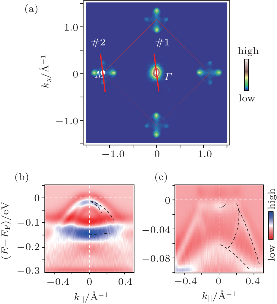
The first characteristic of single-layer FeSe/STO observed by ARPES studies is the interfacial charge transferring process which induces heavy electron doping in the FeSe. The Fermi surfaces of single-layer FeSe/STO consist of only electron pockets [Fig. 3(a)], which is similar to AxFe2− ySe2 (A = K, Cs, Rb, etc.).[34] Thus single-layer FeSe/STO can be classified to the type of heavily electron-doped Fe-based superconductors (called e-FeHTSs hereafter).[35] The absence of hole Fermi surface is distinct from most Fe-based superconductors[31] including bulk FeSe.[35– 39] Around the Brillouin zone center, a parabolic band (band α ) locates below the Fermi energy around the Brillouin zone center, with the band top at − 80 meV [Fig. 3(b)]. Around the Brillouin zone corner, the circular pockets are formed by two nearly degenerate electron bands [Fig. 3(c)]. Estimated from the Luttinger volume, the electron doping is 0.12 e− per Fe for well post-annealed single-layer FeSe/STO.[8, 9] Since single-layer FeSe films are stoichiometric on STO with a perfect lattice and no vacancies as observed by STM studies, [4] the heavy electron doping in single-layer FeSe/STO is induced by the interface.
 | Fig. 3. (a) The Fermi surface mapping of FeSe/STO. (b) The second derivative of the photoemission intensity with respect to energy around the Brillouin zone center, along cut #1 as illustrated in panel (a). (c) The second derivative of the photoemission intensity with respect to energy around the Brillouin zone corner, along cut #2 as illustrated in panel (a). Panel (a) is reprinted with permission from Ref. [9], copyright 2012 by Nature Materials. |
To answer how the interface induces such heavy electron doping, Tan et al. took photoemission data at each step during the growth of 1 ML FeSe film [Fig. 4], which demonstrates the charge transfer from the oxygen deficient STO substrate.[9] The STO substrate shows insulator/semiconductor behavior without density of state (DOS) near Fermi energy [Fig. 4(a)]. After heat treatment in a vacuum, oxygen vacancies appear in STO which induce localized states with high DOS and clear metal-like Fermi-step [Fig. 4(b)]. After the growth of single-layer FeSe, the DOS is again depleted near Fermi energy with the disappearance of Fermi step [Fig. 4(c)], suggesting that the electrons in the localized oxygen-vacancy-induced states are transferred to the FeSe layer, and is responsible for the electron doping in single-layer FeSe. Further studies are needed to resolve why electrons transfer in such a spontaneous way at the interface.
 | Fig. 4. (a)– (c) The photoemission intensity taken around normal emission for the STO substrate after degassing at 550 ° C for 3 h, the STO substrate after 30 min heat treatment at 950 ° C under a Se flux, and 1 ML FeSe, respectively. Panels (a)– (c) are reprinted with permission from Ref. [9], copyright 2012 by Nature Materials. |
However, there are some discrepancies between ex-situ and in-situ ARPES studies. After inadequately-annealing on the Se-capped single-layer FeSe/STO, ex-situ APRES measurements observed a nonsuperconducting phase, [8] which is not observed by in-situ ARPES studies.[9, 10] The observation of the nonsuperconducting phase is probably due to the lower electron doping level in the inadequately annealed Se-capped single-layer FeSe/STO.[8] After adequate post-annealing, ex-situ ARPES measurements show the superconducting phase, and the electron doping increases with a longer annealing period and higher annealing temperature, [8] probably due to the variation of Se content or oxygen vacancies. Thus the charge doping in single-layer FeSe could be tuned by the annealing process, and higher electron doping corresponds to higher superconducting pairing temperature in single-layer FeSe, suggesting that charge doping in FeSe plays an important role in tuning the interfacial superconductivity.[5, 8]
The second characteristic of single-layer FeSe/STO revealed from the photoemission measurement is the full epitaxy of single-layer FeSe on STO, resulting in the large biaxial strain in single-layer FeSe. The symmetry of photoemission intensity map is known to follow the Brillouin zone of the crystal lattice, by inverting which, one can estimate the in-plane lattice constant. Using this method, Tan et al. reported that the in-plane lattice of single-layer FeSe on STO is 3.90 Å , [9] following the in-plane lattice of STO. The same in-plane lattice is estimated in another ARPES study.[7] Compared with the in-plane lattice of bulk FeSe which is 3.765 Å , the in-plane lattice of single-layer FeSe/STO is expanded by 3.7%. Theoretically, it is suggested that single-layer FeSe shows a large mechanical flexibility to support an enormous strain limit up to 30%, [22] which allows further engineering on the tensile strain in single-layer FeSe by using different substrates.
As a third characteristic, evidence for interfacial electron– phonon coupling is revealed by ARPES measurements. Lee et al. clearly observed replica bands in the photoemission spectra of single-layer FeSe/STO, which is explained as the shaking-off bands due to the interactions of electrons in FeSe with a phonon mode in STO across the interface.[10] The energy separation between the main bands and the replica bands is 100 meV, which can be reproduced by theoretical calculations considering the electrons of FeSe couple with a 80 meV flat phonon band. The presence of replica band was further confirmed by Peng et al., [15] with the same energy separation between the main band and the replica band in single-layer FeSe/STO. Based on the simulation in Lee et al., the electron phonon coupling would facilitate Cooper pairing and enhance Tc. It provides a clue for further enhancing Tc by tuning the phonons in the oxide layer, and calls for further experiments to resolve the relationship between Tc and interfacial phonon mode.
For the electron bands around the Brillouin zone corner, ARPES studies reveal a gap around 15 meV at 25 K, [8, 9] with the characteristics of Bogliubov quasiparticle dispersion [Fig. 5(a)]. The gap gradually decreases with the increase of temperature, and eventually closes [Fig. 5(b)]. The gap versus temperature curve is well fitted by the BCS formula, which indicates the superconducting pairing temperature around 65 K [Fig. 5(c)]. The reported superconducting gap closing temperatures are consistent in independent ARPES measurements, which are 65± 5 K, [8] 60± 5 K, [9] and 58± 7 K.[10] Compared with the superconducting transition temperature of 8 K in FeSe bulk crystals, the pairing temperature in single-layer FeSe/STO is significantly enhanced, providing strong evidence on the high Tc in single-layer FeSe/STO.
 | Fig. 5. (a) The band dispersion near Fermi momentum (kF) for single-layer FeSe/STO in the superconducting state. The spectra are symmetrized with respect to the Fermi energy. (b) Temperature dependent behavior of symmetrized spectra. (c) Temperature dependent gap-size and BCS fitting. Panels (b) and (c) are reprinted with permission from Ref. [9], copyright 2012 by Nature Materials. |
STS studies clearly indicate the disappearance of superconductivity in the second layer FeSe/STO.[4] ARPES studies reveal how the electronic structure evolves with the thickness of FeSe.[9, 10] The electronic structures of thick FeSe films are distinct from that of single-layer FeSe/STO. For multi-layer FeSe films, there is spectral weight at Fermi energy around the Brillouin zone center [Fig. 6(a)], which is contributed by several parabolic bands near the Fermi energy [Fig. 6(b)]. These bands do not cross the Fermi energy in the 2 unit-cell (uc) FeSe films[10] and in the 3 uc FeSe films[9] (the slight variation of the critical film thickness is probably due to the different thickness calibrations in these two papers), and gradually shift up and form larger hole pockets in thicker films.[9] Around the Brillouin zone corner, the Fermi surfaces are in a cross shape [Fig. 6(a)], which is formed by the complicated band structure [Fig. 6(c)].
 | Fig. 6. (a) The Fermi surface mapping of 3 uc FeSe/STO. (b) The second derivative of the photoemission intensity with respect to energy around Brillouin zone center, along cut #1 as illustrated in panel (a). (c) The second derivative of the photoemission intensity with respect to energy around Brillouin zone corner, along cut #2 as illustrated in panel (a). Panels (a)– (c) are reprinted with permission from Ref. [9], copyright 2012 by Nature Materials. |
As observed by Tan et al., the band structure [Figs. 7(a)– 7(c)] and the Fermi surfaces [Fig. 7(d)] show strong reconstruction as a function of temperature.[9] With temperature increasing, the separated bands gradually become degenerate above a certain critical temperature, which is 125 K for 50-uc-thick FeSe films as shown in Figs. 7(a) and 7(b). The bands around the Brillouin zone center also slightly shift as a function of temperature [Figs. 7(c)]. In analogy with other Fe-based superconductors such as BaFe2As2 and NaFeAs, the reconstruction of electronic structure is suggested to be short range nematic fluctuation or SDW fluctuation.[9] Recently, similar band splitting behavior has been observed in FeSe bulk crystals, [36, 38, 39] and also verified in FeSe thick films.[40] Due to the absence of magnetic transition in bulk FeSe, [41] and the absence of SDW-fluctuation-induced band folding in ARPES studies, [9, 40] the temperature-dependent behavior of the electronic structure is now generally considered as the electronic nematic transition.[36, 38– 40] The driving force for the nematic transition is suggested to be spin fluctuations, [39, 42] orbital/charge fluctuations[40] or a combination of these two.[36, 38]
 | Fig. 7. (a1)– (a7) The second derivative with respect to energy for the photoemission intensity around the Brillouin zone corner for 50 uc FeSe. (b) The second derivative of the energy distribution curves (EDCs) at Brillouin zone corner. The dip of the second derivative highlights the band position. (c) The second derivative with respect to energy for the photoemission intensity around the Brillouin zone center at 30 K and 135 K, respectively. (d) The photoemission intensity map at 30 K and 135 K, respectively. Panels (a)– (d) are reprinted with permission from Ref. [9], copyright 2012 by Nature Materials. |
At the lowest temperature, the band splitting around the Brillouin zone corner decreases with increasing thickness of the films. Consequently the critical temperature of the nematic transition gradually decreases, suggesting weaker nematicity in thicker FeSe films [Figs. 8(a) and 8(b)]. Following the similar trend, the in-plane lattice constant of FeSe gradually decreases in thicker films [Fig. 8(c)]. By plotting the critical temperatures of the nematic transition as a function of lattice constant, together with the bulk FeSe phase diagram under hydrostatic pressure, [43] Tan et al. obtained a comprehensive phase diagram similar to other Fe-based superconductors with the in-plane lattice as the control parameter [Fig. 8(d)].[9] Superconductivity arises when SDW fluctuations and/or nematicity are suppressed in FeSe. Following this phase diagram, if the single-layer FeSe is freestanding and with the in-plane lattice of STO substrate, it should present the strongest SDW fluctuations or nematicity without superconductivity. However in contrast, the otherwise pronounced SDW fluctuations or nematicity is totally killed in single-layer FeSe/STO with highly enhanced superconductivity compared with bulk FeSe. One possibility is that the heavy electron doping due to charge transfer from the STO substrate [Fig. 3] kills the SDW fluctuations/nematicity, and brings out superconductivity.[9]
 | Fig. 8. (a) Band separation and (b) critical temperature of the nematic transition. (c) In-plane lattice constant of FeSe derived from the inversion of Brillouin zone size as a function of FeSe thickness. (d) Phase diagram of FeSe combining the parameters in panels (a)– (c) and the bulk FeSe phase diagram under hydrostatic pressure. Panels (a)– (d) are reprinted with permission from Ref. [9], copyright 2012 by Nature Materials. |
Based on the characteristics of single-layer FeSe/STO, there are several possible scenarios on the origin of the interfacial superconductivity. One scenario is based on the antiferromagnetic interaction/spin fluctuations-mediated superconductivity, which is currently the dominating picture for bulk Fe-based superconductors.[44, 45] Tensile strain enhances antiferromagnetic interaction, [9, 23] while heavy electron doping due to charge transfer kills the long range order.[23] Superconductivity is enhanced with the enhanced spin fluctuation and suppressed long range order.[9, 23] Based on this scenario, further enhancement of Tc could be realized with further enhanced strain and similar charge transfer. Another scenario suggests that the superconducting pairing is mediated by strong electron– phonon interactions. Superconductivity could be induced by the strong interaction between electrons in FeSe layer and high-frequency phonons in Nb:SrTiO3.[17] Based on this scenario, tuning the phonon mode in the oxide layer would effectively affect superconductivity.
It is crucial to find the key factors among various interfacial interactions [Fig. 9(a)], for both further enhancing Tc and understanding the mechanism of the interfacial superconductivity. The combination of thin film growth and in-situ spectroscopic study provides a powerful approach in studying the dominant interactions, by independently manipulating the epitaxial strain, interfacial oxide, and charge doping in FeSe/oxide [Fig. 9(b)] and studying the corresponding evolution of electronic structure and superconductivity. Using this technique, Peng et al. reported the direct manipulations on different interfacial interactions.
 | Fig. 9. (a) Illustration of the epitaxial strain and charge transfer at the FeSe/oxide interface, and the lattice relaxation and chemical doping in thick FeSe films. (b) Illustration of modifying the epitaxial strain and chemical composition of the oxide layer. (c1)– (c4) The illustration of heterostructures designed for tuning the epitaxial strain and changing the composition of the FeSe/oxide interface in Ref. [15]. |
To study the effect of tensile strain, the heterostructure FeSe/STO/KTaO3 (noted as FeSeSX) was fabricated, which further enhances the lattice constant of FeSe by another 2% to that of KTaO3 (3.989 Å ), without changing the charge transfer and the FeSe/STO interface.[16]
Alternatively, one could preserve the strain by using the same substrate, while changing the oxide adjacent to FeSe, which would vary the screening strength and/or phonon mode at the FeSe/oxide interface.[15] Peng et al. reported the study on FeSe/BaTiO3/KTaO3 with in-plane lattice (3.989 Å ) (noted as FeSeBU), which is identical to the in-plane lattice of with FeSeSX. The FeSeBU and FeSeSX are shown to have the same amount of charge transfer, and form a control group with the composition of interfacial oxide as the clean control parameter.[15]
On the other hand, the surface reconstruction of BaTiO3 induced another type of FeSe film, which matches the 3 × 3 reconstructed BTO lattice with slightly expanded in-plane lattice of 3.78 Å and rotation of 18.5° (noted as FeSeBR). Thus the FeSeBU and FeSeBR form another comparative group with epitaxial strain as the clean control parameter at FeSe/BaTiO3 interface.[15] Therefore, four types of single-layer FeSe/oxide can be studied and compared, to study the dependence of Tc on strain and interfacial oxide materials [Fig. 9(c)].
Similar to single-layer FeSe/STO, the Fermi surfaces of FeSeSX also consist of only electron pockets [Figs. 10(a1) and 10(a2)]. With enhanced tensile strain, the estimated carrier doping does not change, while the shape of the Fermi surfaces is modified. The electron pockets at the zone corner become elliptical in FeSeSX, unlike the circular Fermi surfaces in single-layer FeSe/STO. The enhanced tensile strain in FeSeSX gives rise to more separated γ 1/γ 2 bands [Fig. 10(b1)]. The bandwidths of the electron bands are similar in FeSeSX and single-layer FeSe/STO [Figs. 10(c1) and 10(c2)].
 | Fig. 10. (a1) and (a2) The photoemission intensity map at Fermi energy for FeSeSX and single-layer FeSe/STO, respectively. (b1) and (b2) The separated and degenerate γ bands of FeSeSX and single-layer FeSe/STO, respectively. (c1) and (c2) The replica band of γ band observed in FeSeSX and single-layer FeSe/STO, respectively. The EM indicates the energy separations between the main band and the replica band, which represents the energy scales of the phonon modes. (d1) and (d2) The second derivative image of spectra around zone center, showing the hole-like band α and flat band ω , for FeSeSX and single-layer FeSe/STO, respectively. (e1) and (e2) Comparison of DFT calculations and experimental band dispersions around zone center, for FeSeSX and single-layer FeSe/STO, respectively. Panel (a) is reprinted with permission from Ref. [16], copyright 2014 by the American Physical Society. Panels (b)– (e) are reprinted with permission from Ref. [15], copyright 2014 by Nature Communications. |
Besides, the enhanced epitaxial strain in FeSeSX slightly reduced the energy of the phonon mode that couples with FeSe bands. As shown in Figs. 10(c1)and 10(c2), the energy separation between band γ and its replica varies from 98 meV for single-layer FeSe/STO to 87 meV for FeSeSX.
Around the Brillouin zone center, the expanding of in-plane lattice parameter in FeSeSX was reflected by the narrowing of band α . As shown in Figs. 10(d1) and 10(d2), the band α of FeSeSX becomes flatter and the energy separation between band α and ω decreases. The mass enhancement of band α in enhanced tensile strained films is fully accounted for by density functional theory (DFT) calculations under a renormalization factor of 5.0 [Figs. 10(e1) and 10(e2)]. Therefore, the quasiparticle bandwidth narrowing with enhanced tensile strain could be fully attributed to a pure band effect, that is, the decrement of the hopping integral t.
For another comparative sample of FeSeBU and FeSeBR, the electronic structure shows similar evolutions with tensile strain as in the FeSe/STO interface. The FeSeBR with slight tensile strain shows circular electron pockets around the zone corner, whereas the electron pockets become elliptical in the extremely strained FeSeBU [Figs. 11(a1) and 11(a2)]. The degeneracy of bands γ 1 amd γ 2 is lifted by enhanced tensile strain in FeSeBU compared with FeSeBR [Figs. 11(b1) and 11(b2)]. Around the zone center, the more tensile strained FeSeBU also band mass enhancement of band α compared with FeSeBR [Figs. 11(c1) and 11(c2)]. These results demonstrate that the characteristics of electronic structure dependent on tensile strain.
 | Fig. 11. (a1) and (a2) The photoemission intensity maps and LEED patterns of FeSeBU and FeSeBR, respectively. (b1) and (b2) The separated and degenerate γ bands for FeSeBU and FeSeBR, respectively. (c1) and (c2) The second derivative image of spectra around zone center, showing the hole-like band α and flat band ω , for FeSeBU and FeSeBR, respectively. Panels (a)– (c) are reprinted with permission from Ref. [15], copyright 2014 by Nature Communications. |
The FeSeSX and FeSeBU share the same in-plane lattice constant, the same electron doping judging from Luttinger volume, but differs in the composition of the interfacial oxide. Comparing their electronic structure, the momentum splitting of electron bands is larger in FeSeBU [Figs. 10(b1) and 11(b1)] around the Brillouin zone corner, indicating that the electronic structure of single-layer FeSe is affected by the interfacial oxide material.
Around the zone center, FeSeSX shows flatter band α and smaller band separation between band α and band ω [Figs. 10(d1) and 11(c1)]. The band separation [Fig. 12(a)] and band mass [Fig. 12(b)] as a function of lattice constant fall on different curves for FeSe on STO and FeSe on BTO, respectively, which indicates a non-trivial effect from the different interfacial oxide compositions. Comparing the DFT calculation with the experimental dispersion of band α , the renormalization factor is 4.1 for FeSeBU, which is smaller than that of FeSeSX and single-layer FeSe/STO [Figs. 12(c) and 12(d)]. Therefore, the bandwidth variations for single-layer FeSe films on different oxides are beyond the pure lattice-expansion effect, and there are additional correlation effects that depend on the interface.[15]
 | Fig. 12. (a) The δ E (the energy seperation between band α and band ω at γ as defined in Figs. 10(d) and 11(c)) as a function of lattice constant. (b) The effective mass m* of band α as a function of lattice constant, where me is the mass of free electron. (c)– (d) Comparison of DFT calculation and experimental band dispersion around zone center of FeSeBU and FeSeSX, respectively. Panels (a)– (d) are reprinted with permission from Ref. [15], copyright 2014 by Nature Communications. |
Figures 13(a) and 13(b) show the temperature dependence of the superconducting gap in the four different single-layer FeSe/oxides. For both FeSe/STO and FeSe/BaTiO3 interfaces, large superconducting gaps are observed at low temperature. The gap-closing temperature can be determined by BCS formula.[15] The gap-closing temperatures are slightly enhanced with larger tensile strain and preserved interface, which are enhanced from 65 K in single-layer FeSe/STO to 70 K in FeSeSX, and from 70 K in FeSeBR to 75 K in FeSeB. On the other hand, the gap-closing temperatures are generally higher in films with FeSe/BaTiO3 interface than those with the FeSe/STO interface. The gap-closing temperature of 75 K for FeSeB, and this one set the new pairing temperature record, for both Fe-based superconductors and monolayer films. For these four FeSe films and KxFe2− ySe2, the relationship between gap closing temperature Tδ and the gap amplitude Δ 0 falls on a general linear trend of 2Δ 0 = 6.0kBTg [Fig. 13(c)], where kB is the Boltzmann constant. This indicates the relatively strong coupling superconductivity and the similar superconducting nature in these materials.[15]
 | Fig. 13. (a) The superconducting gap size as a function of temperature and the corresponding BCS fitting for single-layer FeSe/STO and FeSeSX, respectively. (b) The same as panel (a) but for FeSeB and FeSeBR, respectively. (c) The maximal low-temperature gap versus superconducting gap closing temperature, for various FeSe/oxide films and bulk KxFe2− ySe2. Panel (a) is reprinted with permission from Ref. [16], copyright 2014 by the American Physical Society. Panels (b)– (c) are reprinted with permission from Ref. [15], copyright 2014 by Nature Communications. |
In FeSe/STO, the electron doping induced by the interfacial charge transfer[9] is constrained in the first unit cell of FeSe adjacent to the STO.[46] Doping thick FeSe films by chemical substitution allows studying the effect of charge doping on superconductivity without the interfacial effect such as electron– phonon coupling, and with tunable tensile strain which is controlled by the thickness of FeSe.
Peng et al. reported in-situ ARPES study on heavily electron doped 35 uc Fe0.92Co0.08Se (FeCoSeSR) films.[15] Due to the electron carrier introduced by Co doping, the hole like bands α and β in thick FeSe films[9] sink below Fermi energy [Fig. 14(a)]. The nematic order is suppressed by the electron doping as indicated by the simple electron band without splitting around the zone corner [Fig. 14(b)]. The Fermi surfaces consist of only electron pockets [Fig. 14(c)], similar to the Fermi surfaces of the single layer FeSe films on STO and on BaTiO3. The Brillouin size corresponds to an in-plane lattice constant of 3.78 Å , indicating a slight tensile strain identical to that in FeSeBR.
 | Fig. 14. (a) The second derivative with respect to the energy of the photoemission intensity around the Brillouin zone center for 35 uc Co-doped FeSe/STO. (b) The photoemission spectra around the Brillouin zone corner. (c) Photoemission intensity map at Fermi energy, which is integrated over (EF + 10 meV, EF − 10 meV). (d) The symmetrized EDCs around the Fermi momentum of the electron pocket around the Brillouin zone corner at 30 K. Panels (a)– (d) are reprinted with permission from Ref. [15], copyright 2014 by Nature Communications. |
The tensile strain and heavy electron doping in FeCoSeSR are similar to those in FeSeBR, whose superconducting gap-closing temperature is above 70 K.[15] Though the electron doping of 0.08 in FeCoSeSR is lower than that of single layer FeSe/oxides, the simple electronic structure around the zone corner indicates the full suppression of nematic order. If the superconductivity had been originated only from the FeSe layer, a higher superconducting gap-closing temperature would be expected in FeCoSeSR due to the suppressed quantum fluctuation in thicker films. However, in contrast, superconducting gap is absent in FeCoSeSR down to 30 K [Fig. 14(d)]. The metallic state of FeCoSeSR without superconductivity is more likely an over-doped state in bulk Fe-based superconductors, where heavy electron doping kills the superconductivity. Therefore, the combination of electron doping and tensile strain could not account for high temperature superconductivity in FeSe, while oxide interface plays a dominate role in the high temperature superconductivity.
The artificial engineering on the epitaxial strain and interfacial oxide composition induce systematic change of effective mass around the Brillouin zone center, varied band degeneracy around the Brillouin zone corner, and slightly different energy scales of the phonon modes. The electron doping in thick films leads to a metallic state with suppression of nematicity, but without superconductivity. Investigating the effect of these factors on the superconductivity helps to elucidate the mechanism of the interfacial superconductivity.
Based on the spin fluctuation mediated superconductivity, tensile strain would enhance superconductivity if long range order is suppressed.[23] Experimentally, as summarized in Fig. 15(a), the gap-closing temperature is slightly enhanced by tensile strain. Neverthless, the gap-closing temperature is enhanced by 5 K with 5.5% enhancement of in-plane lattice from FeSeBR to FeSeB, which are surprisingly small in the context of the antiferromagnetic interaction/spin fluctuation induced superconductivity. Correspondingly, the significant pairing temperature enhancement from 8 K in bulk FeSe to 65 K in single-layer FeSe/STO could not be accounted by 3.7% enhancement of in-plane lattice. These results suggest that the tensile strain imposed by oxide layer is a positive but not a major factor for the interfacial superconductivity in FeSe/oxide. On the other hand, although with the same in-plane lattice parameter and similar charge doping, the gap-closing temperature is significantly enhanced from FeCoSeSR to FeSeBR. Interfacial interactions beyond epitaxial strain or charge transfer play a dominant role in the interfacial superconductivity.
 | Fig. 15. Superconducting gap closing temperature Tg as a function of in-plane lattice constant a. According to Ref. [15], the Tg of FeCoSeSR is expected to be around 4 K, with the error bar between 0 K and 30 K. (b) Superconducting gap closing temperature as a function of the effective mass me of band α at the zone center. (c) Superconducting gap closing temperature versus the energy scale of the phonon mode represented as EM. Panels (a)– (c) are reprinted with permission from Ref. [15], copyright 2014 by Nature Communications. |
The oxide interface and strain modify the effective mass of band α in single layer FeSe. As shown in various series of Fe-based superconductors, the bandwidth or electronic correlation plays an important role in the superconductivity.[47] However, the gap-closing temperatures do not monotonically correlate with the quasiparticle mass of the α band [Fig. 15(b)]. This could be understood by considering that band α does not contribute to Cooper pairing since it is fully occupied and located well below Fermi energy.[15] The partially occupied electron-like bands show almost an identical bandwidth for different interfacial oxides and tensile strain, which may relate to the robust high pairing temperature in different FeSe/oxide films.
Replica bands near the zone corner were generally observed in single-layer FeSe/oxide with high pairing temperatures, [15] while vanishing in 2 uc FeSe/STO, [10] suggesting that electron-phonon coupling is possibly related to the interfacial superconductivity. The energy scale of phonon mode (EM) deduced from the energy shift of replica bands varies with different interfacial oxides and tensile strain. However, figure 15(c) rules out the direct correlation between the EM and the gap-closing temperature. Further experiments are required to study whether the gap-closing temperature is related to electron– phonon coupling strength or the combination of coupling strength and the ferroelectric phonon energy.
Determining the pairing symmetry helps to resolve the microscopic mechanism of superconductivity. Due to the absence of hole Fermi surface in e-FeHTSs, [35] the pairing symmetry in these materials challenges the prevailing s± pairing, [34] and has been a key unsolved problem in the research of Fe-based superconductor. Theoretically, various scenarios have been proposed, including plain s wave, [48− 51] and different sign-changing scenarios[52– 61] which suggest the sign-reversal of the superconducting gap between different Fermi surface sections along the two electron pockets around the Brillouin zone corner. However, the two electron pockets are nearly degenerate and hard to distinguish in the currently known e-FeHTSs (including AFe2Se2[34] and single layer FeSe/oxide[7, 9]), and nearly isotropic distribution of the superconducting gap distribution has been demonstrated by ARPES, [34, 62] therefore, the different pairing scenarios could not be tested.
As reported by Peng et al., the degeneracy of the electron bands is lifted by the enhanced tensile strain in FeSeSX (Ref. [16]), generating two elliptical Fermi pockets at the zone corner [Fig. 16(a)]. Thus FeSeSX serves as an ideal material to test the pairing symmetry. Along the intersect momentum of the two electron pockets, as demonstrated by the single peak line shape in momentum distribution curves, there is no hybridization between the two electron bands [Figs. 16(b) and 16(c)]. Remarkably, the superconducting gap size is finite at different momentum, and varies along the Fermi surface [Fig. 16(d)]. The momentum distribution of superconducting gap shows a four-fold symmetry, but without a node [Fig. 16(e)].
 | Fig. 16. (a) The sketch of Brillouin zone and Fermi surfaces of FeSeSX. (b) The momentum distribution curves showing the dispersion of band γ along cut #1, and the momentum location of #1 is illustrated in panel (a). (c) The fitting of band γ at the Fermi energy along cut #1 by Lorentz peaks. (d) The symmetrized photoemission spectra showing the evolution of the superconducting gap as a function of polar angle φ as defined in panel (a). (e) Gap distribution of the electron pocket in polar coordinates, where the radius represents the gap size and the polar angle represents φ . Panels (a)– (d) are reprinted with permission from Ref. [16], copyright 2014 by the American Physical Society. |
The anisotropic but nodeless gap distribution poses constraints on scenarios of different superconducting pairing symmetries. The bonding-antibonding s± and d+ is scenarios[60, 61] are based on the strong hybridization between the two electron pockets, which are not observed in FeSeSX. The d-wave[52, 53] and orbital anti-phase s± scenarios[58, 59] without hybridization would unavoidably induce node, which are absent in the experimental data.[16] Additional inter-band s-wave pairing could lift the node with a finite gap size, [56, 57] resulting in the gap anisotropy. Alternatively, the anisotropic but nodeless gap distribution could be induced by the anisotropic Fermi surface topology or orbital dependent gap size with sign preserving s-wave pairing.[48– 51] To further resolve the remaining scenarios, it is crucial to determine the sign of the order parameter by phase sensitive experiments.
The phase information of superconducting gap can be deduced though magnetic field dependent STS measurement and analysis on the quasiparticle interference (QPI). The scattering potentials induced by vortices would enhance the sign-preserving scatterings and suppress the sign-changing ones.[63, 64] By measuring the single layer FeSe/STO, Fan et al. observed an overall suppression of QPI intensity around the superconducting gap energy for all the scattering vectors, [6] indicating the similar sign structure of Bogoliubov quasi-particle scattering involving different electron pockets.
The response of the superconductivity to local impurities also reflects the phase information of the superconducting gap.[65] According to Anderson’ s theorem, in a plain-s-wave pairing superconductor, magnetic impurities other than non-magnetic impurities would suppress superconductivity.[55, 56] However, for the phase-changing pairing, such as d-wave or s± -wave pairing, both magnetic and non-magnetic impurities would suppress superconductivity and induce in-gap states.[67] In the STS study, Fan et al. observed in-gap states and supressed superconducting coherence peaks around the site of magnetic impurities, while the superconducting gap kept undisturbed around the site of non-magnetic impurities.[6] Therefore, the combination of all these results suggests a plain s wave as the pairing symmetry in the single-layer FeSe/oxide.
From interface engineering, the interfacial interaction between FeSe and oxides is proven to play a dominant role in the high Tc. The absence of the FeSe/oxide interface would remove high temperature superconductivity although with a similar strain and electron doping.[15] If the glue for Cooper pairing in the single layer FeSe/oxide is spin fluctuation, which is the dominant picture in bulk Fe-based superconductors, there should be a non-trivial enhancement of spin fluctuation by the FeSe/oxide interface, but beyond the tensile strain effect.[15] For example, the interfacial electron– phonon interaction could possibly enhance the spin fluctuation in single-layer FeSe according to theoretical calculations.[10]
Alternatively, the superconductivity could be entirely induced by the FeSe/oxide interface with different mechanisms from Fe-based superconductors. The Cooper pairing may be mediated by electron– phonon interactions as in conventional superconductors. For single-layer FeSe/oxide, it is proposed that the high-frequency phonon modes in Nb:SrTiO3 or Nb:BaTiO3 may mediate superconductivity, [17] and strong electron– phonon interaction is evident from the replica band behavior in single-layer FeSe/oxide.[10, 15] Indeed, conventional superconductors could show very high Tc with high frequency phonons and strong electron– phonon coupling, as recently demonstrated in H2S under high pressure.[68] The scenario with electron– phonon interaction as the pairing mechanism is also supported by the ARPES and STS measurements indicating plain s wave pairing symmetry.[6] Nevertheless, smoking gun experiments are required to directly resolve whether Tc binds with the interfacial electron– phonon coupling. Besides, further studies are required to resolve the role of interfacial electron– phonon coupling to determine the pairing glue.
Looking into the future, the research on single-layer FeSe/oxide is still in its infancy, and there is much more to be resolved. For example, following the interface engineering results, more oxides with a distinct optical phonon can be explored to grow single-layer FeSe in the future, which may also hopefully further enhance Tc. Moreover, combining the in-situ transport measurement with interface engineering would benefit in accurately pinning down the Tc in various FeSe/oxides and searching for higher Tc in more FeSe/oxide systems. Fabricating and measuring superconducting junctions of FeSe/oxide would deepen our understanding on the property of interfacial superconducting and give rise to possible practical applications.
To summarize, we have reviewed some recent progresses on single-layer FeSe/oxide through the combined studies of in-situ spectroscopic measurements and atomic scale engineering. Although we are still far from reaching a definite conclusion on the glue of pairing at the FeSe/oxide interface, the combined engineering and probing techniques provide important insights in resolving the effect of various interactions and studying the pairing symmetry, which set constraints on possible scenarios of the interfacial superconductivity. The superconducting pairing temperature has been enhanced to 75 K. These progresses pave the ways for future studies to unveil the superconducting mechanism and to search for higher Tc.
We gratefully acknowledge Prof. Qikun Xue, Prof. Xi Chen, and Dr. Wei Li for sharing their recipe of growing FeSe films, Xin Xie, Xia Lou for substrate prepration, Dr. Shiyong Tan, Qin Fan, Prof. Tong Zhang, Qi Song, Chenhaoping Wen, Yujia Pu, Zican Huang for the sample growth and spectroscopic measurements, and many collaborators for their helpful discussion.
| 1 |
|
| 2 |
|
| 3 |
|
| 4 |
|
| 5 |
|
| 6 |
|
| 7 |
|
| 8 |
|
| 9 |
|
| 10 |
|
| 11 |
|
| 12 |
|
| 13 |
|
| 14 |
|
| 15 |
|
| 16 |
|
| 17 |
|
| 18 |
|
| 19 |
|
| 20 |
|
| 21 |
|
| 22 |
|
| 23 |
|
| 24 |
|
| 25 |
|
| 26 |
|
| 27 |
|
| 28 |
|
| 29 |
|
| 30 |
|
| 31 |
|
| 32 |
|
| 33 |
|
| 34 |
|
| 35 |
|
| 36 |
|
| 37 |
|
| 38 |
|
| 39 |
|
| 40 |
|
| 41 |
|
| 42 |
|
| 43 |
|
| 44 |
|
| 45 |
|
| 46 |
|
| 47 |
|
| 48 |
|
| 49 |
|
| 50 |
|
| 51 |
|
| 52 |
|
| 53 |
|
| 54 |
|
| 55 |
|
| 56 |
|
| 57 |
|
| 58 |
|
| 59 |
|
| 60 |
|
| 61 |
|
| 62 |
|
| 63 |
|
| 64 |
|
| 65 |
|
| 66 |
|
| 67 |
|
| 68 |
|