Indium–tin oxide films obtained by DC magnetron sputtering for improved Si heterojunction solar cell applications*
Gu Jin-Hua

, Si Jia-Le, Wang Jiu-Xiu, Feng Ya-Yang, Gao Xiao-Yong, Lu Jing-Xiao
Key Laboratory of Materials Physics of Ministry of Education, School of Physical Engineering, Zhengzhou University, Zhengzhou 450052, China
†Corresponding author. E-mail: gujinh@zzu.edu.cn
*Project supported by the National High Technology Research and Development Program of China (Grant No. 2011AA050501).
1. IntroductionIndium– tin oxide (ITO) films are generally used as the front electrodes in heterojunction (HJ) solar cells due to their lower resistivity and high transmittance.[1– 3] The ITO films can be deposited by various techniques, such as sol– gel, [4, 5] chemical vapor deposition (CVD), [6] electron beam evaporation, [2] pulsed laser deposition, [7] direct-current (DC) magnetron sputtering, [8] and radio-frequency (RF) magnetron sputtering.[3, 9] The DC magnetron sputtering technique is one of the most effective methods since this method has a high deposition rate and the ITO films prepared have high stability and excellent performance. The transparency and conductivity of the ITO films are critically dependent on the deposition conditions. Depositing highly conductive and transparent ITO films is a key to obtaining excellent HJ solar cells. To obtain the high-quality ITO films for Si HJ solar cell application, we studied the effects of the deposition parameters on the properties of ITO in DC sputtering, and ITO films with lower resistivity of 4× 10− 4 Ω · cm and high transmittance of 89% were obtained with a high sputtering power of 110 W. However, for preparing the Si HJ solar cell, the ion bombardment upon the p layer will take place during the ITO deposition process. Due to the quite thin p layer with a total thickness of about 10 nm, [10] the ion bombardment upon the p layer will influence the performance of the HJ solar cell. Study about this topic has not been reported. In this paper, we discuss the influence of the ion bombardment upon the p layer on the performance of the Si HJ solar cell when ITO is deposited with a high sputtering power. To check the quality of the c-Si surface passivation by a-Si(i):H, the performances of the solar cells with and without an intrinsic a-Si:H layer are compared. The Voc is improved from 0.626 V to 0.673 V when the 5 nm thick intrinsic a-Si:H layer is inserted. The higher Voc of 0.673 V for the single-side HJ solar cell implies the excellent c-Si surface passivation by a-Si:H.
2. Experimental details2.1. Fabrication of ITO thin filmsITO thin films were prepared by DC magnetron sputtering. The ITO target material contained 90 wt.% of In2O3 and 10 wt.% of SnO2. The base pressure in the chamber was 2.0 × 10− 3 Pa. The distance between the target and the substrate was about 65 mm. The substrate was a float glass. The reaction gas was an argon and oxygen mixture. The argon flow rate was 20 sccm, and the oxygen flow rate was in the range of 0– 0.7 sccm. The other deposition parameters were as follows: substrate temperature of 200 ° C, sputtering power of 50– 110 W, and sputtering pressure of 0.4– 1.2 Pa. The thickness of ITO was measured using ellipsometry. The optical transmittance was measured using a UV– visual spectrophotometer. The sheet resistance of the ITO films was measured using the four-point probe method.
2.2. Si HJ solar cell fabricationITO/ (p) a-Si:H/ (i) a-Si:H/ (n) c-Si /Al single-side solar cells were fabricated on n-type (100) Cz polished Si substrates with the resistivity of 1– 10 Ω · cm. The p-type a-Si:H was deposited using radio frequency plasma enhanced chemical vapor deposition (RF-PECVD). The a-Si(i):H was deposited using very high frequency plasma enhanced chemical vapor deposition (VHF-PECVD). The thicknesses of the (p) a-Si:H layer and the a-Si(i):H layer are about 15 nm and 5 nm, respectively. The 80 nm thick ITO as the front electrodes and antireflection layer was deposited on the (p) a-Si:H by DC magnetron sputtering. The Al electrodes were deposited on the back surface by evaporation. The area of the solar cell is 0.25 cm2.
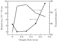
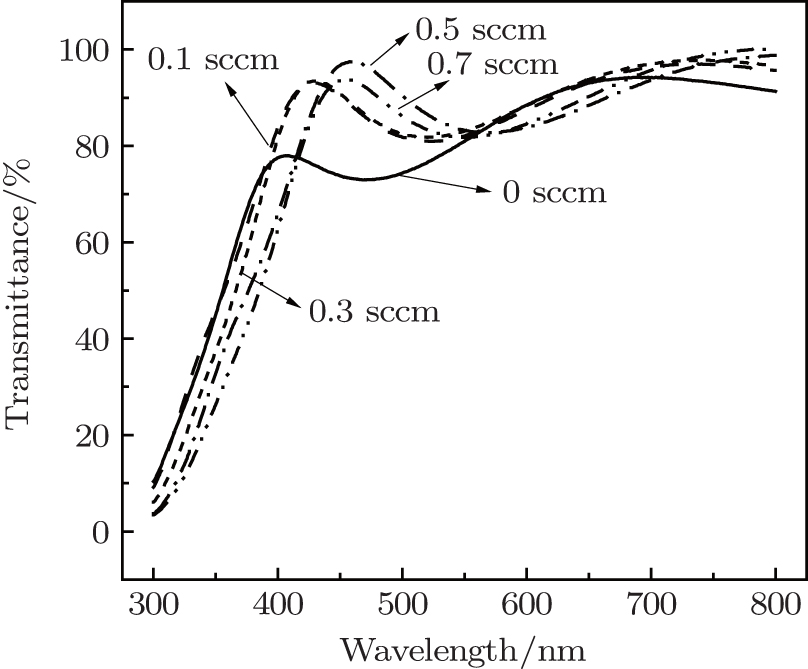
3. Results and discussion3.1. Effect of the oxygen flow rate on the properties of ITO thin filmsFigure 1 shows the transmittance spectra of ∼ 200 nm thick ITO films deposited with different oxygen flow rates. When the oxygen flow rate is 0 sccm, the indium and tin are not fully oxidized, the transmittance is lower. When the oxygen flow rate increases to 0.1– 0.3 sccm, the indium and tin are fully oxidized, so ITO has a high transmittance. When the oxygen flow rate is 0.5– 0.7 sccm, excess oxygen atoms lead to not-transparent oxide, which results in the decrease of the transmittance of the ITO thin films.
Figure 2 shows the variation of the resistivity of the ITO films with the oxygen flow rate. When the oxygen flow rate is high, excess oxygen atoms will fill in the oxygen vacancies and result in the increase of the resistivity of the ITO thin films. When the oxygen flow rate is 0.1– 0.3 sccm, the indium and tin are fully oxidized and the number of oxygen vacancies is proper, then ITO has the high transmittance and low resistivity, i.e., resistivity of 4× 10− 4 Ω · cm and average transmittance of 89%.
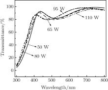
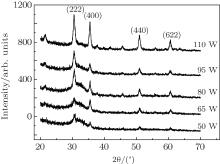
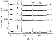
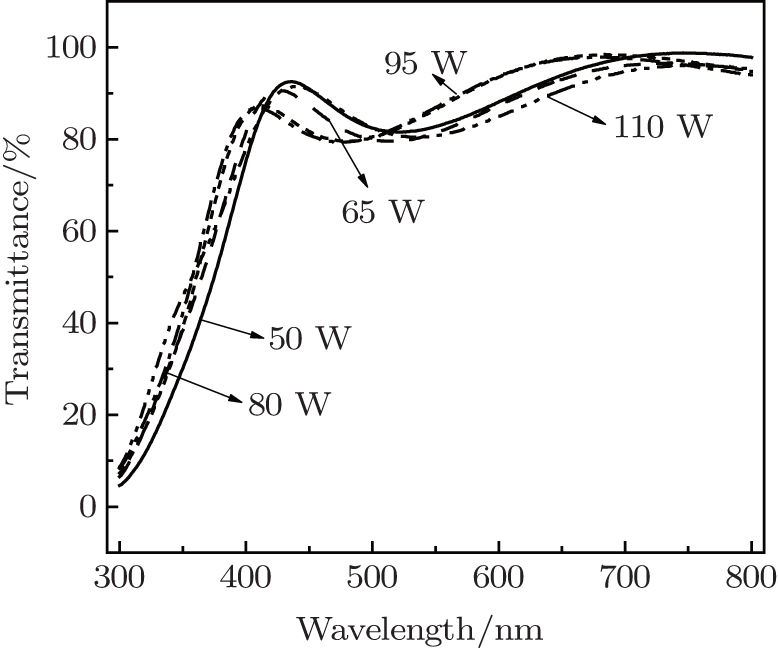
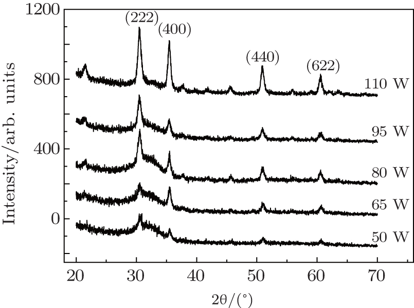
3.2. Effect of the magnetron power on the properties of ITO thin filmsThe transmittance spectra and resistivity of 200 nm thick ITO films deposited with different sputtering powers are shown in Figs. 3 and 4. When the sputtering power is low (50 W), the transmittance is low and the resistivity is high. The reason is that as the energy of the sputtered atoms is low, they are difficult to react with oxygen, then the indium and tin are not fully oxidized, so the transmittance of ITO is low. On the other hand, the sputtered atoms do not have enough energy to migrate on the substrate surface, so the crystallization is low (as can be seen in the XRD of Fig. 5), thus the conductivity of ITO is low. When the sputtering power increases, the energy of the sputtered atoms increases, the indium and tin fully react with oxygen, then the transmittance increases. On the other hand, the sputtered atoms have enough energy to migrate on the substrate surface, so the crystallization is high (as can be seen in the XRD of Fig. 5), which increases the conductivity of ITO. When the sputtering power is 110 W, the resistivity is 4× 10− 4 Ω · cm and the average transmittance is over 89%.
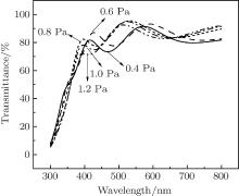
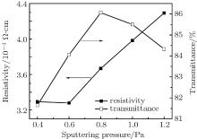
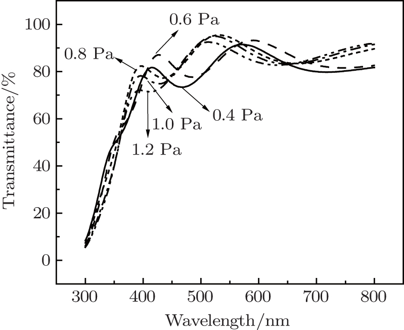
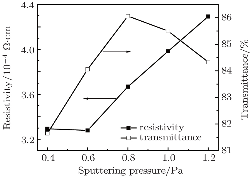
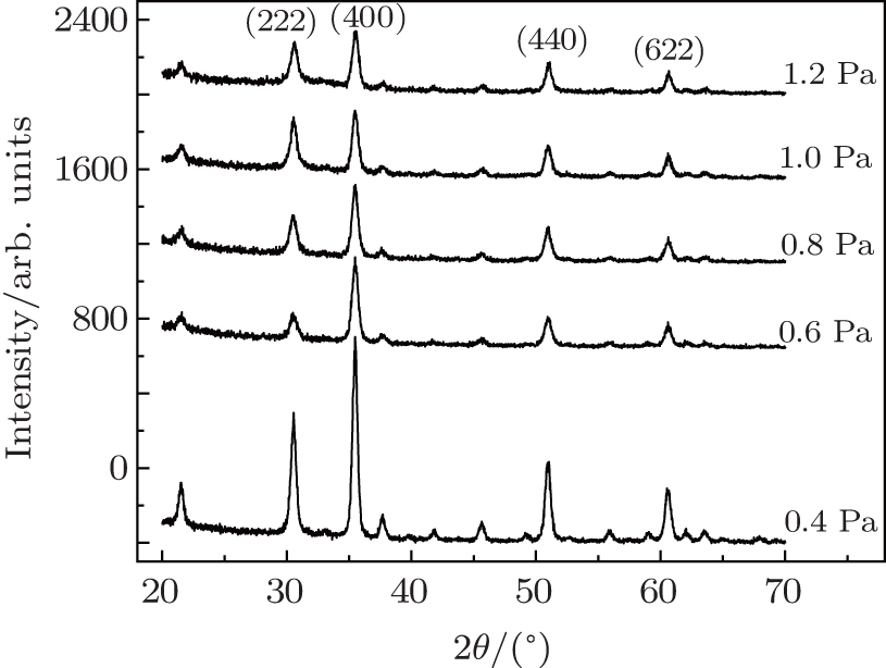
3.3. Effect of the magnetron pressure on the properties of ITO thin filmsFigures 6 and 7 give the transmittance spectra and resistivity of ∼ 270 nm thick ITO films deposited under different sputtering pressures. It can be seen that when the sputtering pressure is 0.4 Pa, the transmittance is about 82%. The transmittance increases as the pressure increases. When the pressure is over 0.8 Pa, the transmittance begins to decrease. The reason is that when the sputtering pressure increases, the collision between the sputtering atoms increases, the indium and tin react more fully with oxygen, so the transmittance increases. When the sputtering pressure is even higher, Ar+ being strongly scattered results in the decrease of the energy of the sputtering atoms, so the crystallization is lower (as can be seen in the XRD of Fig. 8), thus the transmittance and conductivity of ITO decrease. The increase of the resistivity of ITO under high pressure is ascribed to the decrease of the crystallization (as can be seen in the XRD of Fig. 8). Considering the transmittance and conductivity of ITO, the optimized pressure is 0.8 Pa.
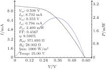
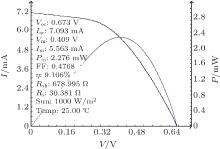
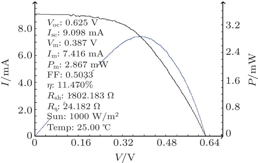
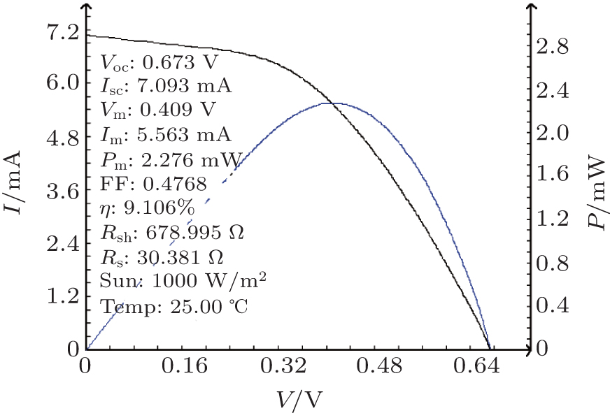
3.4. The application of ITO thin films in the Si HJ cellsUnder the optimized condition, i.e., the oxygen flow rate is 0.1 sccm, the pressure is 0.8 Pa, and the sputtering power is 110 W, the high quality ITO with low resistivity of 4× 10− 4 Ω · cm and high transmittance of 89% is obtained. Figure 9 shows the I– V characteristic of the solar cell without an intrinsic buffer layer fabricated with the optimized ITO. The Voc of 0.598 V is obtained for the single-side HJ solar cell without an intrinsic a-Si:H buffer layer. To decrease the ion bombardment to the p layer in the HJ solar cell, ITO is deposited with lower sputtering power of 95 W. Figure 10 gives the I– V characteristic of the solar cell fabricated with ITO under 95 W sputtering power. We can see that the Voc is improved to 0.626 V and the efficiency reaches 11.47%. Consider the ion bombardment to the p layer during the ITO deposition, a little decrease of the sputtering power is beneficial to improving the performance of the HJ solar cell. To reduce the interface recombination between the p layer and the c-Si, a 5 nm thick intrinsic a-Si:H layer is inserted, the I– V characteristic of the solar cell with the intrinsic a-Si:H layer is shown in Fig. 11. The Voc is improved to 0.673 V owing to the excellent c-Si surface passivation by the intrinsic a-Si:H. However, the efficiency and Jsc of the solar cell with the (i) a-Si:H layer clearly decrease, the reason is that the a-Si(i):H layer is probably a little thicker than 5 nm (the thickness is difficult to control due to the high depposition rate of a-Si(i):H using VHF-PECVD). The high resistivity of the (i) a-Si:H layer increases the series resistance, thus the effeciency and Jsc of the solar cell decrease. Although the highest efficiency of our solar cell is only 11.47%, this is an encouraging result for the single-side HJ solar cell without metal grid line and back field.
4. ConclusionHigh quality ITO films with resistivity of 4× 10− 4 Ω · cm and average transmittance of 89% in the wavelength range of 380– 780 nm were grown by DC magnetron sputtering at the substrate temperature of 200 ° C. The optimized ITO films were used to fabricate the single-side HJ solar cell. For the single-side HJ solar cell without intrinsic a-Si:H buffer layer, the highest conversion efficiency was 11.47% with Voc of 0.626 V. The Voc was improved to 0.673 V when a 5 nm thick intrinsic a-Si:H layer was inserted between the (p) a-Si:H and (n) c-Si layer. The higher Voc of 0.673 V of the single-side HJ solar cell implies the excellent c-Si surface passivation by a-Si:H. This is an encouraging result for future fabrication of highly efficient HJ solar cells.


