Electronic properties of the SnSe–metal contacts: First-principles study
Dai Xian-Qia), b)  , Wang Xiao-Long
a) , Li Weia) , Wang Tian-Xinga)
, Wang Xiao-Long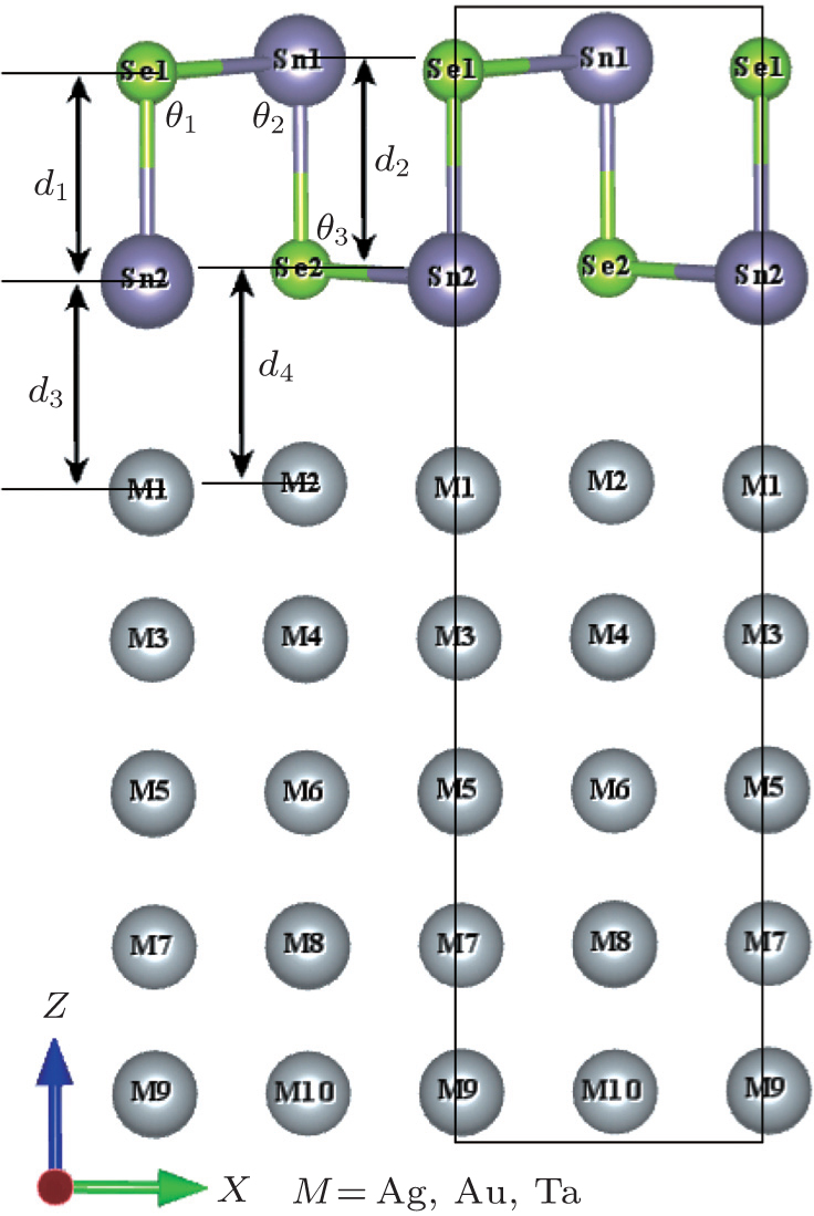
Electronic properties of the SnSe–metal contacts: First-principles study |
|
Dai Xian-Qi
, Wang Xiao-Long |
| Side view of monolayer SnSe absorbed on M(001) substrates. θ 1, θ 2, θ 3, and θ 4 represent the angles Sn2–Se1–Sn1, Se1–Sn1–Se2, Sn1–Se2–Sn2, and Se2–Sn2–Se1, respectively. d 1, d 2, d 3, and d 4 represent the Se1–Sn2 bond length, Sn1–Se2 bond length, the interface distance between Sn2 and the metal surface, and the interface distance between Se2 atom and the metal surface, respectively. Se1, Sn1 and Se2, Sn2 are classified as the top and bottom layers, respectively. The black frame stands for the unit cell of the SnSe/metal contact. |
| |