

Electronic properties of the SnSe–metal contacts: First-principles study*
[Dai Xian-Qia), b)  , Wang Xiao-Long
a) , Li Weia) , Wang Tian-Xinga) ]
, Wang Xiao-Long|
|


†Corresponding author. E-mail: xqdai@htu.cn
*Project supported by the National Natural Science Foundation of China (Grant Nos. U1304518 and U1404109).
The geometries and electronic properties of SnSe/metal contact have been investigated using first-principles calculation. It is found that the geometries of monolayer SnSe were affected slightly when SnSe adsorbs on M ( M = Ag, Au, Ta) substrate. Compared with the corresponding free-standing monolayer SnSe, the adsorbed SnSe undergoes a semiconductor-to-metal transition. The potential difference Δ V indicates that SnSe/Ta contact is the best candidate for the Schottky contact of the three SnSe/M contacts. Two types of current-in-plane (CIP) structure, where a freestanding monolayer SnSe is connected to SnSe/M, are identified as the n-type CIP structure in SnSe/Ag contact and p-type CIP structure in SnSe/Au and SnSe/Ta contact. The results can stimulate further investigation for the multifunctional SnSe/metal contact.
Over the past years, metal– semiconductor contacts[1– 4] have attracted considerable attention in both experimental and theoretical fields, and many capabilities and performances have already been achieved. However, with the development of the nano-device, one of the key issues in nanotechnology is to control the material size at the nanoscale. Therefore, there has been an increased demand for understanding the electronic properties of the nano-scale metal– semiconductor contact to achieve desired functional materials with quantum engineering. Many important properties of materials in technological applications, such as contact in micro- and nano-electronics[5, 6] and thermoelectric devices, [7] are strongly affected by the presence of interfaces. The importance of interfaces lies in the fact that they induce a broad range of novel effects that are not found in the bulk materials.
Recently, Zhao et al.[8] reported that an unprecedented ZT of 2.66 ± 0.3 at 923 K was realized in SnSe single crystals measured along the b axis of the room-temperature orthorhombic unit cell. As a typical IV– VI group semiconductor, SnSe is a p-type semiconductor[9] and belongs to the orthorhombic crystal system which resembles a distorted NaCl structure.[10] Bulk SnSe has an indirect band gap of 0.9 eV, [11] which is the best band gap scope for solar cells, while SnSe nanostructured thin films possess an indirect band gap of 1.5 eV.[12] Similar to other group IV-VI binary semiconductors such as GeSe, SnS, and GeS, the bonding of SnSe interacts covalently within the layer, which comprises zig-zag double layer planes of the selenium and tin atoms and is separated by weak van der Waals force between the layers.[13– 15] Up to now, SnSe semiconductor has been prepared by several techniques such as brush plating, [16] vacuum thermal evaporation, [17] electro deposition, [18, 19] chemical vapor deposition, [20] and laser ablation.[21] Moreover, the monolayer SnSe has been prepared by pulse electrodeposited on tin oxide coated glass substrates at different duty cycles.[22] Due to its potential applications and optoelectronic properties as holographic recording systems, memory devices, radiation detectors, materials for solar cells, [23] it has been widely studied.
In this work, we present a systematic first-principles study on the SnSe/M contact. We firstly obtain the most stable structures. The charge density difference investigates the charge redistribution at the interface. The interface interaction mainly derived from the p or d orbital of atoms in the vicinity of the interface. The potential difference Δ V and CIP structure show the properties of SnSe/M contact as a rectifying junction. The rest of the paper is organized as follows. In Section 2, we summarize the computational details. The results and discussion are present in Section 3. Finally, the conclusions will be given in Section 4.
The calculations are based on density functional theory (DFT), [24, 25] using the projector-augmented plane wave (PAW) method, [26, 27] as implemented in the Vienna ab initio simulation package (VASP).[28, 29] To treat electron exchange and correlation, we choose the Perdew– Burke– Ernzerhof (PBE)[30, 31] generalized-gradient approximation (GGA) which can yield the correct ground-state structure of the combined systems. The cutoff energy is chosen to be 500 eV for the plane-wave basis set. The geometry optimization was carried out using a 9 × 9 × 9 Monkhost– Pack k-points grid.[10] The lattice constants of metals and free-standing monolayer SnSe were obtained by structure relaxation. To investigate the SnSe/metal contact, we have chosen a supercell that contains a slab of five layers of metal atoms, monolayer SnSe sheet and a 15 Å vacuum region to eliminate the interaction between periodic images. For the structure optimization, we fixed the atoms in the two bottom metal layers at their respective bulk position, while all other atoms are fully relaxed until the residual force on each atom is smaller than 1 × 10− 2 eV/Å , and the energy convergence criteria of 1 × 10− 5 eV is met.
Recently, the successful fabrication of monolayer SnSe provides an opportunity to design SnSe/metal junction by contacting metal with SnSe. Hence, the monolayer SnSe constructed in this article is reasonable. The optimized lattice constants of monolayer SnSe are a = b = 4.32 Å , which are in good agreement with the experimental value (a = b = 4.29 Å ).[22] In the following calculations, we use the optimized lattice constants.
For the candidates to the substrate, we consider metals with a lattice plane that can match the SnSe structure because a large mismatch induces strain to distort SnSe. After going through the periodic table, we choose metals Ag, Au, and Ta as candidates for the SnSe/metal contact, the optimized lattice constants are a = b = c = 4.1 Å , 4.1 Å , 4.23 Å , respectively, which have relatively minimal lattice mismatch with SnSe. For each candidate of SnSe/metal contact, there are three different initial configurations to be investigated: the (001), (110), and (111) surfaces. The total energy relaxation results show that the monolayer SnSe can only perfectly match with Ag(001), Au(001), and Ta(001) surfaces without significant Sn– Se bond distortion (as shown in Fig. 1). The metal surface atoms are nearly in the same plane without significantly protruding. Since the three metals are all face-centered cubic, each atom of the SnSe bottom layer can stand nearly on the top site of the metal atoms. The calculated equilibrium bond angles (θ ), bond lengths (d), and binding energies for all the SnSe/metal contacts are summarized in Table 1.
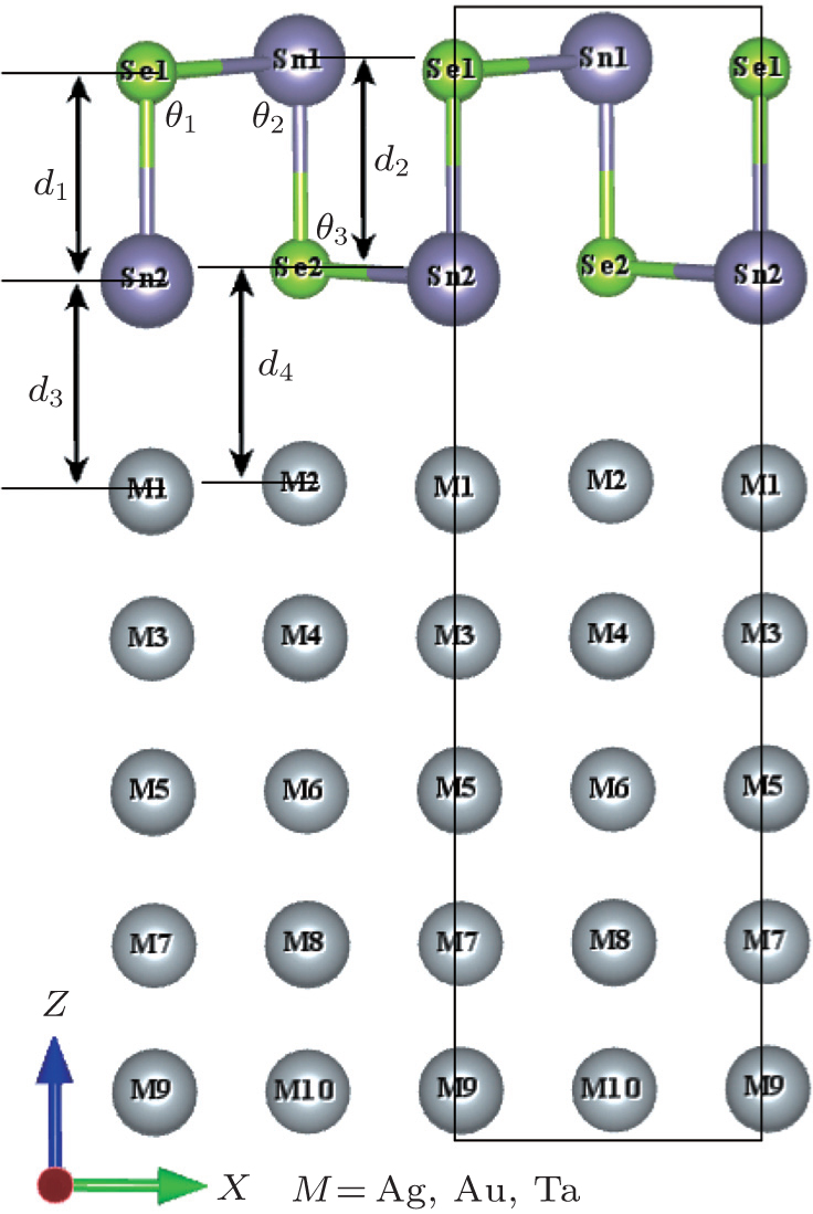 | Fig. 1. Side view of monolayer SnSe absorbed on M(001) substrates. θ 1, θ 2, θ 3, and θ 4 represent the angles Sn2– Se1– Sn1, Se1– Sn1– Se2, Sn1– Se2– Sn2, and Se2– Sn2– Se1, respectively. d1, d2, d3, and d4 represent the Se1– Sn2 bond length, Sn1– Se2 bond length, the interface distance between Sn2 and the metal surface, and the interface distance between Se2 atom and the metal surface, respectively. Se1, Sn1 and Se2, Sn2 are classified as the top and bottom layers, respectively. The black frame stands for the unit cell of the SnSe/metal contact. |
| Table 1. The structure data (see Fig. 1) and the binding energy Eb. |
The binding energy Eb of monolayer SnSe on M substrate is calculated by

where ESnSe− sub is the total energy of the SnSe/M contact, ESnSe and Esub are the total energies of free-standing monolayer SnSe, and the metal substrate, respectively, and n is the number of SnSe primitive cells in the super structure. The calculated binding energies of SnSe adsorbed on the Ag, Au, and Ta substrates are 0.50 eV, 0.67 eV, and 1.24 eV, respectively.
As shown in Table 1, the structure data of SnSe/M vary according to the species of metals. Compared to free-standing monolayer SnSe, the maximum change of θ 1 is − 3.54° in SnSe/Au contact and that of θ 3 is − 3.56° in SnSe/Ag contact. The maximum change of θ 2 is − 1.44° in SnSe/Ag contact, while it is + 1.47° in SnSe/Ta contact for θ 4. The bond length d1 and d2 are slightly larger than that of freely monolayer SnSe (2.73 Å ). Clearly, the geometric structure of monolayer SnSe is affected slightly.
In order to visualize the tendencies of the charge redistribution, we calculate charge density difference

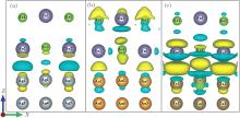
where ρ SnSe − sub, ρ SnSe, and ρ sub are the total charge density of SnSe/metal contacts, monolayer SnSe, and metal substrate, respectively. As shown in Fig. 2(a), it is only weak perturbation at the interface of SnSe/Ag contact. For the SnSe/Au contact (Fig. 2(b)), a strong charge depletion and accumulation for the bottom atoms Sn2 and Se2, respectively, and the top atoms Sn1 and Se1 are also affected significantly. Compared to SnSe adsorbed on the Ag and Au substrate, the charge transfer is the strongest in the interface for SnSe/Ta contact (Fig. 2(c)), which is well consistent with the calculated binding energy.
 | Fig. 2. Charge density difference for the (a) SnSe/Ag, (b) SnSe/Au, and (c) SnSe/Ta contacts, respectively. Yellow regions represent the charge accumulation, and blue regions represent the charge consumption. |
Although the contour plots corresponding to the three substrates are different, a further inspection reveals some common tendencies. In each case only electrons of the surface layer of metal are perturbed by the interface formation, leaving the deeper layers practically unchanged. The electrons spilling into the interface region are mainly derived from p and d orbitals.
In order to analyze the effect of charge redistribution on monolayer SnSe, we calculate the total density of states (TDOS) of SnSe. As shown in Fig. 3, the occupied states of free-standing monolayer SnSe lie around three energy zones, namely, from − 14.2 to − 12 eV, from − 8 to − 5.5 eV, and from − 5.5 to − 0.4 eV with respect to the Fermi level (Ef). For simplicity, we labeled the three occupied states as peak I, II, and III, respectively. Due to the large interfacial dipole shift associated with the considerable charge transfer, the peaks of monolayer SnSe below the Ef show different characteristics after adsorption. The peaks I and II are shifted down to lower energies by around 0.3 and 0.7 eV, respectively, while the peak III is extended widely, which implies that the electrons have been more delocalized. The density of states at Ef are about 0.17, 0.32, and 0.52 (states/eV unit cell) for the SnSe adsorbed on the Ag, Au, and Ta substrate, respectively. SnSe undergoes a semiconductor-to-metal transition in the semiconductor/metal contact.
 | Fig. 3. Total density of state for SnSe, the black line, light gray line, dark orange line, and dark olive line represent the freely monolayer SnSe, the SnSe adsorbed on Ag, Au, Ta substrate, respectively. The Fermi level is set to zero and marked by a dotted line. |
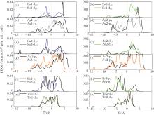
For comprehensiveness, we have investigated the partial density of states (PDOS) of the three systems. Figure 4 plots the PDOS which makes the main contribution to the interaction, the PDOS of Ag(Au) in SnSe/Ag(Au) and Sn2, Se2, in SnSe/Ta are shifted towards the lower energy by 1– 2 eV with respect to Ef (Figs. 4(c), 4(g), 4(i), 4(k)). This is mainly attributed to the charge redistribution and the interface repulsive electrostatic potential. In the SnSe/Ag(Au) contact, the Ag(Au) only interacts strongly with the Sn2 atom, while in the SnSe/Ta contact, the Ta atom not only interacts strongly with the Sn2 atom, but also interacts strongly with the Se2 atom. This result can explain why the SnSe/Ta contact has the maximum binding energy.
 | Fig. 4. Partial density of state for the SnSe/metal contacts (a)– (d) for Ag substrate, (e)– (h) for Au substrate, (i)– (n) for Ta substrate. The black lines and color lines stand for before adsorption and after adsorption, respectively. The Fermi level is set to zero and marked by a dotted line. |
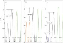
Note that metal and monolayer SnSe have different electrostatic potentials in their isolated states; we calculate the distributions of planar-averaged potential of the SnSe/M systems (Fig. 5). The peaks of averaged potential appear at the middle of each two neighboring atomic layers. We only investigate the potential difference Δ V using the formula Δ V = VI − VM, where VM is the highest averaged potential at the metal surface, and VI is the highest averaged potential at the contact interface. The results are summarized in Table 2. All the results are positive and the SnSe/Ta contact has the maximum potential difference, the similar case is found in Zn-phosphorus contact.[32] Though there is a nonzero TDOS at the Fermi level, the larger potential difference makes electronic transportation from metal to SnSe hard at the interface. Therefore, the SnSe/M contacts, especially the Ta/SnSe contact, are good candidates for Schottky contact.
 | Fig. 5. Planar-averaged potential along the z axis for (a) Ag-, (b) Au-, (c) Ta-SnSe. Light gray line, dark orange line, and dark olive line represent the Ag, Au, Ta planar-averaged potential, respectively. The black line represents the planar-average potential in the interface, and the lime line represents the SnSe planar-average potential. The black arrows represent the position of atomic layer. SnSe-B and SnSe-T represent the SnSe bottom layer and top layer, respectively. |
| Table 2. The highest averaged potential difference (Δ V) between the metal surface and the contact interface (as shown in Fig. 5), the Fermi-level shift (Δ Ef) of adsorbed SnSe (“ − ” or “ + ” denotes n-type doped or p-type doped). |
In the abundant electronic device, only part of the SnSe sheet covers the metal electrode, i.e., the current-in-plane (CIP) geometry, where the charge transfer takes place in order to accommodate the Fermi level difference. Then alignment of the Fermi levels results in the band bending. However, from the CIP point of view, the band bending influences the property of the semiconductor/metal contact. To estimate the degree of band bending, Khomyakov et al.[33] defined the formula: Δ Ef = W − WSnSe, where the W and WSnSe are the work function of SnSe/metal and freestanding SnSe, respectively. The band bending region is n- or p-type doped, depending on the sign of Δ Ef. If Δ Ef < 0, SnSe is n-type doped, and if Δ Ef > 0, it is p-type doped. As tabulated in Table 2, the SnSe/Au and SnSe/Ta contacts belong to the p-type CIP device, while the SnSe/Ag contact belongs to the n-type CIP device. To check reliability of calculation on the band bending, we have recalculated the band bending by using Heyd– Scuseria– Ernzerhof (HSE) hybrid functional and obtained Δ Ef = − 0.25 eV (0.40, 0.22 eV) for the Ag/SnSe (Au/SnSn, Ta/SnSe) contact. Though there are some differences between the results of HSE hybrid functional and that of DFT, the band bending properties in the CIP structure are the same. The type of the CIP device estimated by the DFT level is convinced.
In summary, we have examined the adsorption of monolayer SnSe on Ag(001), Au(001), and Ta(001) surfaces. The geometric structure of monolayer SnSe is affected slightly by the substrates due to the very small lattice mismatch. SnSe/Ta contact is outstandingly more stable over the SnSe/Au and SnSe/Ag contact. The densities of states indicate that the SnSe undergoes a semiconductor-to-metal transition in the SnSe/metal contact. The p or d orbitals of Sn2, Se2, and interfacial metal atoms, which lie around from 0 to − 5 eV, facilitate strongly the interaction between the SnSe and metal substrate. The potential difference Δ V is calculated, and the maximum Δ V is found in the SnSe/Ta contact, which indicates that the SnSe/Ta contact is the best candidate for the Schottky contact. The CIP-structure investigation suggests that the Ag/SnSe contact is an n-type device, while the Au/SnSe and Ta/SnSe contacts are the p-type devices. Our finding may promote the manufacture of the semiconductor/metal contact.
| 1 |
|
| 2 |
|
| 3 |
|
| 4 |
|
| 5 |
|
| 6 |
|
| 7 |
|
| 8 |
|
| 9 |
|
| 10 |
|
| 11 |
|
| 12 |
|
| 13 |
|
| 14 |
|
| 15 |
|
| 16 |
|
| 17 |
|
| 18 |
|
| 19 |
|
| 20 |
|
| 21 |
|
| 22 |
|
| 23 |
|
| 24 |
|
| 25 |
|
| 26 |
|
| 27 |
|
| 28 |
|
| 29 |
|
| 30 |
|
| 31 |
|
| 32 |
|
| 33 |
|