Zhang Sheng, Wei Ke, Yu Le, Liu Guo-Guo, Huang Sen, Wang Xin-Hua, Pang Lei, Zheng Ying-Kui, Li Yan-Kui, Ma Xiao-Hua, Sun Bing, Liu Xin-Yu. AlGaN/GaN high electron mobility transistor with Al2O3+BCB passivation . Chinese Physics B, 24(11): 117307
Permissions
AlGaN/GaN high electron mobility transistor with Al2O3+BCB passivation
Zhang Shenga),b), Wei Keb), Yu Lea),b), Liu Guo-Guob), Huang Senb), Wang Xin-Huab), Pang Leib), Zheng Ying-Kuib), Li Yan-Kuib), Ma Xiao-Huaa), Sun Bingb), Liu Xin-Yub)
School of Advanced Materials and Nanotechnology, Key Laboratory of Wide Bandgap Semiconductor Materials and Devices, Xidian University, Xi’an 710071, China
Microwave Device and IC Department, Institute of Microelectronics, Chinese Academy of Sciences, Beijing 100029, China
In this paper, A12O3 ultrathin film used as the surface passivation layer for AlGaN/GaN high electron mobility transistor (HEMT) is deposited by thermal atomic layer deposition (ALD), thereby avoiding plasma-induced damage and erosion to the surface. A comparison is made between the surface passivation in this paper and the conventional plasma enhanced chemical vapor deposition (PECVD) SiN passivation. A remarkable reduction of the gate leakage current and a significant increase in small signal radio frequency (RF) performance are achieved after applying Al2O3+BCB passivation. For the Al2O3+BCB passivated device with a 0.7 μm gate, the value of fmax reaches up to 100 GHz, but it decreases to 40 GHz for SiN HEMT. The fmax/ ft ratio (≥ 4) is also improved after Al2O3+BCB passivation. The capacitance–voltage ( C– V) measurement demonstrates that Al2O3+BCB HEMT shows quite less density of trap states (on the order of magnitude of 1010 cm−2) than that obtained at commonly studied SiN HEMT.
Many issues still exist in wide applications of AlGaN/GaN HEMT. One major problem is the electron trapping, which restricts the microwave output power and linearity. The traps are located mainly at the semiconductor surfaces/interfaces and in the GaN buffer layer. Deposition of a passivation layer mitigates the contribution from surface traps. PECVD SiN thin films are commonly used for surface passivation, [1, 2] thus improving the performance of the device. However, the SiN passivation technique has faced some serious problems including: i) possible plasma-induced damages to the surface when PECVD is used to deposit SiN[3] films; ii) the contradiction between the current collapse suppression and higher leakage current; [4] iii) the mismatch with GaN makes lots of traps in the SiN, further leading to pinholes. SiN passivation may result in undesired device characteristics, such as higher gate leakage and lower cutoff frequency.
In recent years, some new methods to deal with the surface conditions and new passivation layer, such as Sc2O3, [5, 6] SiO2, [7] MgO, [8] AlN, [9, 10] and Al2O3[11] have been used more frequently. In contrast to the conventional SiN passivation, Al2O3 thin film has more additional benefits, [12] such as a large band-gap (∼ 8.9 eV), thermal stability (amorphous up to at least 1000 ° C), a high breakdown field (5– 10 MV/cm), and chemical stability against GaN, and thus it is a compelling candidate for AlGaN/GaN HEMT passivation.[7, 13] For thermal ALD, water vapor is used as an oxidant and no plasma treatment is needed. Al2O3 deposited by thermal ALD has been demonstrated to have a low defect density, high uniformity, and nanometer scalability. In this paper, a 20-nm Al2O3 passivation layer is deposited on the AlGaN surface, and then heat cured benzo cyclo butane (BCB), which offers good thermal stability and chemical stability, is used to protect Al2O3 from being damaged and polluted.
2. Experiment
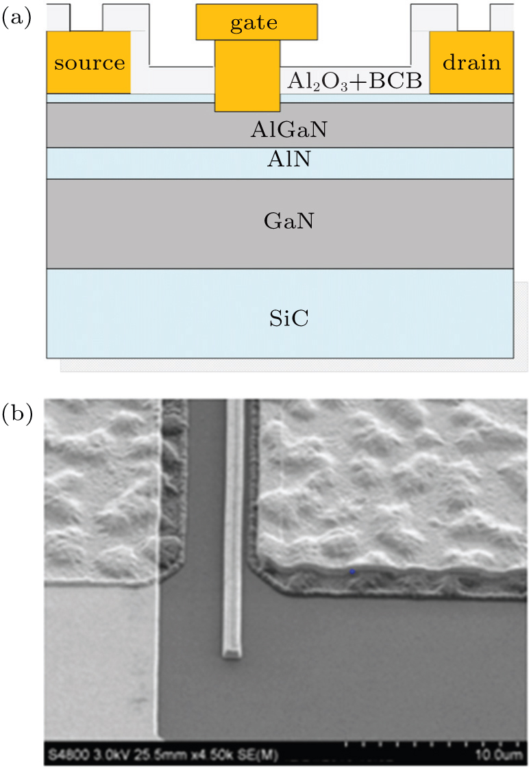
Figure 1 shows the cross section of AlGaN/GaN HEMT. The epitaxial layers were grown on SiC substrate by metal organic chemical vapor deposition (MOCVD) and the heterostructure consists of a 1.5-nm GaN cap layer, 17.6-nm Al0.25GaN, 2-nm AlN, and GaN buffer layer. For the starting material considered here, the sheet resistance (Rsq) values as high as 272.4 Ω /sq and a Hall mobility of 2361 cm2/V− s are demonstrated at room temperature (300 K). The source-drain and gate length are 2.4 μ m and 0.7 μ m, respectively. The process for the GaN HEMT device follows the conventional steps: mesa isolation with N molecules, ohmic metallization with Ti/Al/Ni/Au (= 200/1800/550/450± 100 Å ), annealing at 870 ° C for 50 s by using rapid thermal annealing in nitrogen atmosphere, and it has a contact resistance as low as ρ c = 1.787 × 10− 5 Ω · cm2. The gate metallization Ni/Au (100/3000 Å ) is confirmed with electron beam lithography. To investigate the influence of Al2O3+ BCB passivation on HEMT, the substrate is split into two pieces which are passivated respectively with 200-nm SiN and 20-nm Al2O3. Then 2.7-μ m BCB is deposited on the Al2O3 layer. Reference [13] gave the interface characteristics between Al2O3 and AlGaN/GaN in detail. In the present paper, we ultimately select a thickness of 20 nm, considering the vertical structure of the device and the practical coverage of Al2O3.
Fig. 1. (a) Cross section of AlGaN/GaN HEMT; (b) micrograph of T-gate.
3. Results and discussion
3.1. DC characteristics
We measure DC characteristics for the small gate width of the 50-μ m periphery device by using an HP4155A semiconductor parameter analyzer. Figure 2(a) shows the transfer characteristics of the two devices before and after passivation at Vds = + 6 V. The peak transconductance (Gm) of an unpassivated device is 250 mS/mm and increases to 307 mS/mm after SiN passivation, and it increases to 301 mS/mm after Al2O3+ BCB passivation. Figure 2(b) shows the IV characteristics. The maximum drain current density is 0.82 A/mm for the unpassivated device, it increases to 0.97 A/mm after SiN passivation, and it increases to 1.1 A/mm after Al2O3+ BCB passivation. DC characteristics of devices increase significantly after passivation. In addition, it can be seen that the Gm, in a wide range, keeps a constant, indicating that the device with Al2O3+ BCB passivation shows an outstanding linearity.
Fig. 2. (a) Transfer characteristics of transistors, (b) I– V characteristics of transistors, and (c) the gate leakage current of transistors.
Another important parameter is the gate leakage current. In this case, the drain contact is biased at zero voltage and the gate is swept from 2 V to − 20 V. Two samples after passivation present a significant difference as shown in Fig. 2(c). Negligible increase of the leakage current is found after device passivation with Al2O3+ BCB, while the leakage current increases about one order of magnitude after SiN passivation. Besides, compared with the SiN passivation HEMT, the turn-on voltage of the Al2O3+ BCB passivation HEMT increases slightly. The bigger the turn-on voltage is, the higher the reliability of the device is. It is considered that the suppression of the gate leakage current seems to come from the reaction of the AlGaN surface with oxygen from Al2O3.[14] The surface reaction removes the donor-like traps on the surface and makes the current flow only through the 2DEG channel.[15] Here, the ideal factor of the Schottky contact n is also extracted. For Al2O3+ BCB passivation and SiN passivation, n = 1.87 and 2.1, respectively. The smaller n is related to the low leakage current and the better surface quality.
3.2. RF characteristics
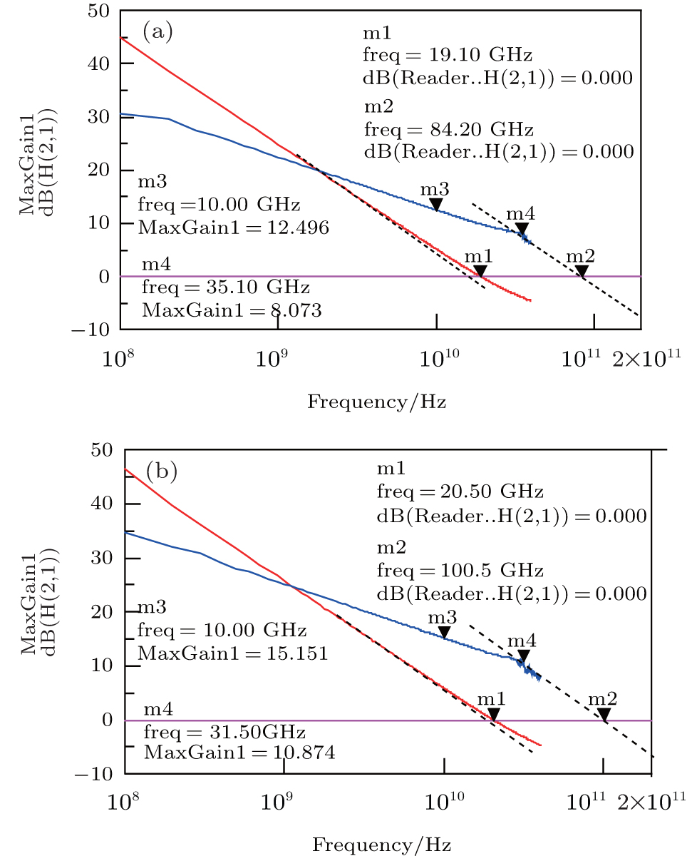
The S parameters of the two devices after passivation with a 50-μ m gate width are measured as a function of frequency and bias by using an Agilent HP8510C Vector Network Analyzer. The corresponding current gain and maximum available gain (MAG) are shown in Figs. 3 and 4. The values of current gain cutoff frequency (ft) are similar (about 20 GHz) for both devices. However, the maximum oscillation frequency (fmax) for the Al2O3+ BCB passivation device is found to be much higher than that of the SiN passivation device. The fmax/ft ratio (≥ 4) changes significantly after Al2O3+ BCB passivation. From these results, it is clear that an enhancement of small signal radio frequency (RF) performance can be achieved after Al2O3+ BCB device passivation. We consider that the density of interface or surface states might be relevant to the RF performance of AlGaN/GaN HEMT and the improved RF performance indicates that Al2O3+ BCB passivation contributes to reducing the surface states and is an excellent passivation technology.
Fig. 4. Small-signal characteristics of SiN passivation HEMT. (a) Vds = 6 V, Vgs = − 1.5 V; (b) Vds = 28 V, Vgs = − 1.5 V.
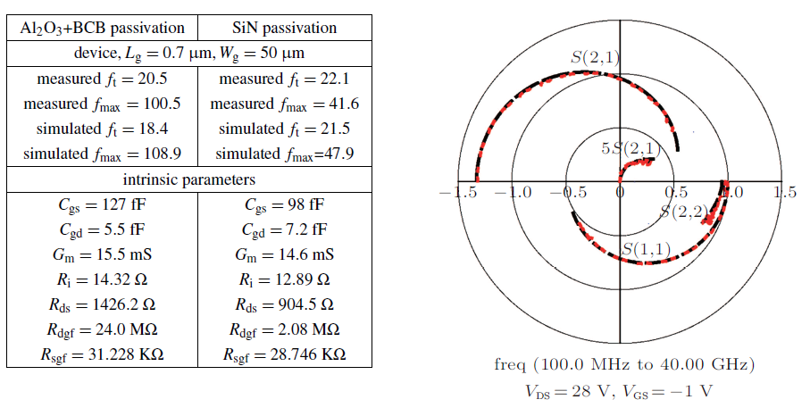
Table 1.
Table 1.
Table 1. Small-signal characteristics of the two devices.
Vds/V
ft/GHz
fmax/GHz
Gain10GHz/dB
Knee freq/GHz
SiN
6
17.0
37.6
11.107
14.0
passivation
28
22.1
41.6
12.511
8.6
Al2O3+ BCB
6
19.1
84.2
12.49
35.1
passivation
28
20.5
100.5
15.151
31.5
Table 1. Small-signal characteristics of the two devices.
To further investigate the RF characteristics of the two devices, small-signal parameters are extracted using a 22-element equivalent circuit model as shown in Fig. 5. It can be found that the simulated data are in good agreement with the measured results, demonstrating the effectiveness of the parameter extraction. Obviously, there are little differences among the values of Gm, Cgs, and Cgd of the two devices, while there exists a significant difference between the two output resistance Rds values. In general, Rds depends on the current flowing through the buffer layer and indicates the quality of the buffer layer. In this paper, the only difference between the two devices is the passivation layer, and Rds could be used to represent the surface and barrier layer, reasonably, implying that the low density of trapping (avoiding plasma-induced damage) causes the current flowing through barrier layer to decrease, and then the Rds for Al2O3+ BCB HEMT to increase. From the following equations:
it follows that the ft values of the two devices are substantially the same; and there is a 58.6% improvement in fmax for Al2O3+ BCB HEMT. The fmax/ft ratio for Al2O3+ BCB HEMT increases about twice, compared with that for the SiN HEMT. Namely, it could enhance the power and gain characteristics by making the Al2O3+ BCB passivation for AlGaN/GaN HEMT work at a higher frequency, but unnecessarily by reducing the gate length. Furthermore, we believe that the different resistances Rgdf and Rgsf, [16] related to the resistances of the gate-to-source and gate-to-drain diodes, are necessary to describe the gate leakage current conduction under the negative gate bias condition, [17] which is meaningful for AlGaN/GaN HEMT. The larger resistance indicates few surface traps and a better Schottky characteristic.
Fig. 5. Intrinsic parameters from determined S parameters.
3.3. C− V measurement
In insulator/semiconductor systems, the electrical characteristics are greatly affected by some charges at the surface or within bulk materials, resulting from native or process-introduced defects. These charges can be determined by C− V measurement.
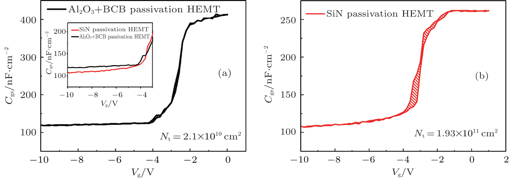
Surface trapped charges can usually be obtained from hysteresis C− V measurement by assuming that all other charges remain unchanged during device operation. The hysteresis C− V curves of the two devices shown in Fig. 6, demonstrate a flat band voltage shift (Δ VFB) in the SiN HEMT and a negligible hysteresis in Al2O3+ BCB HEMT. The shaded area represents the trapped charge quality, and the density (Nt) is calculated by using the following formula:
where q is the electronic charge, Vpinch– off is the pinch-off voltage, and C is the capacitance per unit area. Among the studied devices, SiN HEMT demonstrates a larger trapped charge density of about 1.93 × 1011 cm− 2, and Al2O3+ BCB passivation HEMT possesses better hysteretic characteristics with a trapped charge density of 2.1 × 1010 cm− 2. Additionally, so many charges can cause a serious reverse leakage current, featured by a decrease in reverse capacitance. From the curves in the inset of Fig. 6, Al2O3+ BCB passivation exhibits good ability to block leakage current. The influence of surface trapping on the gate capacitance has been investigated by numerical simulation.[18] Briefly, the channel carrier under the gate is depleted in the off-state and only the fringe capacitance remains there. If there are many traps on the surface close to the gate, they serve as part of the gate and deplete the carriers under the surface, and thus reduce the capacitance.[19]
Fig. 6. (a) C– V characteristics of Al2O3+ BCB passivation HEMT, and the reverse capacitance shown in the inset. (b) C– V characteristics of SiN passivation HEMT.
4. Conclusions
This paper elucidated the influence of Al2O3 deposited by thermal ALD on the AlGaN/GaN HEMT performance. An improvement in the gate leakage current characteristic and RF performance was obtained after device passivation with Al2O3+ BCB as compared with the conventional PECVD SiN passivation. The C– V measurement indicates the promising application of Al2O3+ BCB surface passivation material for GaN-based electronic devices. Especially, the increased fmax/ft ratio indicates that the Al2O3+ BCB passivation is an excellent potential for HEMT in high-frequency and high-power microwave applications.
... PECVD SiN thin films are commonly used for surface passivation,[1,2] thus improving the performance of the device ...
1
2005
0.0
0.0
... PECVD SiN thin films are commonly used for surface passivation,[1,2] thus improving the performance of the device ...
1
2014
0.0
0.0
... However, the SiN passivation technique has faced some serious problems including: i) possible plasma-induced damages to the surface when PECVD is used to deposit SiN[3] films ...
1
2006
0.0
0.0
... [4] iii) the mismatch with GaN makes lots of traps in the SiN, further leading to pinholes ...
1
2004
0.0
0.0
... In recent years, some new methods to deal with the surface conditions and new passivation layer, such as Sc2O3,[5,6] SiO2,[7] MgO,[8] AlN,[9,10] and Al2O3[11] have been used more frequently ...
1
2002
0.0
0.0
... In recent years, some new methods to deal with the surface conditions and new passivation layer, such as Sc2O3,[5,6] SiO2,[7] MgO,[8] AlN,[9,10] and Al2O3[11] have been used more frequently ...
2
2007
0.0
0.0
... In recent years, some new methods to deal with the surface conditions and new passivation layer, such as Sc2O3,[5,6] SiO2,[7] MgO,[8] AlN,[9,10] and Al2O3[11] have been used more frequently ...
... [7,13] For thermal ALD, water vapor is used as an oxidant and no plasma treatment is needed ...
1
2005
0.0
0.0
... In recent years, some new methods to deal with the surface conditions and new passivation layer, such as Sc2O3,[5,6] SiO2,[7] MgO,[8] AlN,[9,10] and Al2O3[11] have been used more frequently ...
1
2012
0.0
0.0
... In recent years, some new methods to deal with the surface conditions and new passivation layer, such as Sc2O3,[5,6] SiO2,[7] MgO,[8] AlN,[9,10] and Al2O3[11] have been used more frequently ...
1
2013
0.0
0.0
... In recent years, some new methods to deal with the surface conditions and new passivation layer, such as Sc2O3,[5,6] SiO2,[7] MgO,[8] AlN,[9,10] and Al2O3[11] have been used more frequently ...
1
2004
0.0
0.0
... In recent years, some new methods to deal with the surface conditions and new passivation layer, such as Sc2O3,[5,6] SiO2,[7] MgO,[8] AlN,[9,10] and Al2O3[11] have been used more frequently ...
1
2008
0.0
0.0
... In contrast to the conventional SiN passivation, Al2O3 thin film has more additional benefits,[12] such as a large band-gap (#cod#x223C ...
2
2011
0.0
0.0
... [7,13] For thermal ALD, water vapor is used as an oxidant and no plasma treatment is needed ...
... [13] gave the interface characteristics between Al2O3 and AlGaN/GaN in detail ...
1
2008
0.0
0.0
... [14] The surface reaction removes the donor-like traps on the surface and makes the current flow only through the 2DEG channel ...
1
2008
0.0
0.0
... [15] Here, the ideal factor of the Schottky contact n is also extracted ...
1
1991
0.0
0.0
... Furthermore, we believe that the different resistances Rgdf and Rgsf,[16] related to the resistances of the gate-to-source and gate-to-drain diodes, are necessary to describe the gate leakage current conduction under the negative gate bias condition,[17] which is meaningful for AlGaN/GaN HEMT ...
1
2010
0.0
0.0
... Furthermore, we believe that the different resistances Rgdf and Rgsf,[16] related to the resistances of the gate-to-source and gate-to-drain diodes, are necessary to describe the gate leakage current conduction under the negative gate bias condition,[17] which is meaningful for AlGaN/GaN HEMT ...
1
2009
0.0
0.0
... [18] Briefly, the channel carrier under the gate is depleted in the off-state and only the fringe capacitance remains there ...
AlGaN/GaN high electron mobility transistor with Al2O3+BCB passivation
[Zhang Shenga),b), Wei Keb), Yu Lea),b), Liu Guo-Guob), Huang Senb), Wang Xin-Huab), Pang Leib), Zheng Ying-Kuib), Li Yan-Kuib), Ma Xiao-Huaa), Sun Bingb), Liu Xin-Yub)]


 , Yu Le