
Electron Raman scattering in semiconductor quantum well wire of cylindrical ring geometry
[Betancourt-Riera Re.a), b)  , Betancourt-Riera Ri.
a) , Nieto Jalil J. M.c) , Riera R.b) ]
, Betancourt-Riera Ri.|
|


†Corresponding author. E-mail: rbriera@gmail.com
We study the electron states and the differential cross section for an electron Raman scattering process in a semiconductor quantum well wire of cylindrical ring geometry. The electron Raman scattering developed here can be used to provide direct information about the electron band structures of these confinement systems. We assume that the system grows in a GaAs/Al0.35Ga0.65As matrix. The system is modeled by considering T = 0 K and also a single parabolic conduction band, which is split into a sub-band system due to the confinement. The emission spectra are discussed for different scattering configurations, and the selection rules for the processes are also studied. Singularities in the spectra are found and interpreted.
Owing to the promising physical features, the low-dimensional semiconductor nanostructures have been widely investigated both experimentally and theoretically.[1, 2] Because of their potential technological applications, in the last decade, there have been many studies on the semiconductor quantum well wire of cylindrical ring geometry. This system is an excellent candidate for various optoelectronic, high temperature, and high-frequency device applications, such as light-emitting diodes, laser diodes, field-effect transistors, solar cells, chemical and biological sensors.[3] Recently, spin-dependent electron transport in the mesoscopic system has attracted considerable attention because of its potential application in a new scientific area, spintronics, where the spin degree of freedom may be utilized to process information.[4] The experimental research on Raman scattering in nanocrystals has been extensively reported.[5– 12] To interpret the experimental results, the theoretical research usually focused on the calculation of the differential cross-section (DCS) for Raman scattering.[13, 14] Thus, the calculation of the DCS for electron Raman scattering (ERS) remains a rather interesting and fundamental issue.[15] Recently, the experimental research on the Raman scattering in the GaN semiconductor quantum well wire of cylindrical ring geometry was reported.[16– 19]
When studying a physical system from the viewpoint of quantum mechanics, the properties of the physical system are contained in the system wave function. In this work, we determine the stationary states of an electron subjected to an external potential to form a semiconductor quantum well wire of cylindrical ring geometry. Besides, as the device has been developed using a GaAs/Al0.35Ga0.65As matrix (the previous works used a matrix of GaN[18, 19]), we can assume that the system has only one conduction band partially filled. We assume a parabolic band for the electron, which is split into a sub-band system due to the confinement, and T = 0 K. This model is commonly used in the II– VI and III– V semiconductors when the description is near the center of the Brillouin zone in the reduced zone scheme. Under these dynamical conditions, and since the potential barriers do not imply interband transitions or the complex valence band of the III– V and II– VI semiconductor compounds, the contribution of band mixing is small in the confinement regime, which is assumed in this work and it is consistent with the previous treatments.[20, 21]
Because of its precision, Raman scattering is a useful technique for studying the electronic structure of nanostructures by considering different polarizations of incident and emitted radiations.[21– 23] The analysis of the DCS of a Raman scattering process allows us to determine the sub-band structure of a nanostructured system by a direct inspection of the singularity positions in the spectra, considering the selection rules of transitions of the carriers participating in the interaction with the incident and emitted light of different polarizations. In general, the DCS shows singularities related to the intersub-band and intraband transitions, in our case, only the intersub-band transitions are considered. The result depends on the scattering configurations, and the structure of singularity depends on the incident or emitted photon polarization. The electron Raman scattering has been studied from a theoretical point of view in various systems, such as quantum well, quantum wire (cross-section with cylindrical disk geometry and also with square geometry), and quantum dot systems. These studies considered the interband and intrasub-band transitions with and without the participation of confinement phonons, also in the presence and absence of external electric and magnetic fields; [24– 34] the bulk semiconductor, considering the presence of electric and magnetic fields, was studied too.[35– 37] Surface enhanced Raman scattering is one of the most powerful probing methods, which is non-destructive, real-time, good at highly sensitive characterization.[38, 39] Raman scattering studies of phonon modes are of fundamental importance for understanding the structural and optical properties, the surface states can lead to novel magnetic properties.[40, 41] In the previous studies, the surface optical phonon mode, which is sensitive to the shell thickness, has been found in core/shell quantum dots and core– shell structured nanoparticles. Recently, it has been proposed to be realized in commonly used semiconductors, which suggests a promising approach to the development of semiconductor electronic devices.[41]
In the present work, we present a model of electron Raman scattering for a semiconductor quantum well wire (QWW) of cylindrical ring geometry. The system can be fabricated with GaAs/Al0.35Ga0.65As by using high-resolution electron-beam lithography techniques. The intersub-band ERS processes can be qualitatively described in the following way: first an electron in the conduction band absorbs a photon of incident radiation of energy ħ ω l, then the electron emits a photon of secondary radiation of energy ħ ω s due to a new intersub-band transition.[42]
Our problem is to determine the stationary states of an electron in a QWW system of cylindrical ring geometry with internal radius ra, external radius rb, and length L. The envelope function approximation leads to the solution of the Schrö dinger equation. The confinement potential is[43]

The solution of the Schrö dinger equation leads to
 |
with the electron energy

where

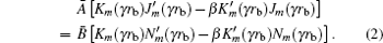
u0 (r) is the electron Bloch function in the band; Jm and Ym are the Bessel functions of the first and the second kind of order m; Im and Km are the modified Bessel functions of the first and the second kind, here we have used the definitions of Bessel functions according to Abramowitz; [44] and μ 1 (μ 2) is the electron effective mass outside (inside) of the QWW. By considering the continuity of the function Ψ and the current density (1/μ )(∂ Ψ /∂ r) at the interface, we can calculate the constants. Then

where
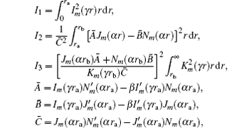
with 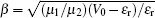
 |
As can be observed, for each value of m, n energy values are obtained. The states are then described by the following quantum numbers: m = 0, 1, … ; n = 1, 2, … ; and kz (see Refs. [32] and [42]).
The Raman differential cross-section in a volume per unit solid angle for incoming light of frequency ω l and scattered light of frequency ω s is given in Refs. [24] and [25], and it can be written as
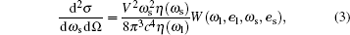 |
where η (ω ρ ) is the refraction index as a function of the radiation with frequency ω ρ ; eρ is the light polarization unit vector; the subindex ρ = l (s) indicates the incident (secondary) radiation; c is the light velocity in a vacuum, and W(ω l, el, ω s, es) is the transition rate for the absorption and emission radiation calculated according to Fermi’ s golden rule
 |
with
 |
Here Ĥ ρ is the Hamiltonian operator for the radiation field, in the dipole approximation, with frequency ω ρ and polarization unit vector eρ , [42] while | i〉 and | f〉 are the initial and the final states with energies Ei and Ef, respectively; and | a〉 and | b〉 are the intermediate states with energies Ea and Eb, whose lifetimes are Γ a and Γ b. In this case, we have two possibilities:[42] (i) the electron absorbs the incident photon and later emits the secondary radiation photon, which is represented by the first term of Eq. (5); (ii) the electron emits the secondary radiation photon and later absorbs the incident photon which is represented by the second term of Eq. (5).
The Hamiltonian operator for the radiation field has the form
 |
where p̂ = − iħ ∇ and μ is the electron effective mass.
The dipole approximation is commonly used in studying electron Raman scattering and resonant Raman scattering in nanostructures. This approximation is valid as long as the radiation wavelength is much longer than the radius of the wire. The effect of reduced dimensionality on the free carrier absorption and the selection rules for intersub-band transition has been discussed in Ref. [42], and there it is shown that the ERS can only take place in the confinement direction, then

where

Now we must calculate the matrix elements appearing in Eq. (4). We use the condition k = 0 for the radiation field; [24, 42] thus, by considering Eqs. (1) and (6), the following matrix elements are obtained:
 |
where 


and μ 0 is the electron free mass. The explicit forms of Im′ m″ and IIm′ m″ are very complicated and their expressions can be calculated following the method reported in Ref. [42]. As can be observed, the emission or absorption of one photon can only take place between consecutive states of the quantum numberm according to the selection rule m″ = m′ ± 1, while there is no restriction on quantum number n (see Eq. (7)).
In the initial state, we have an electron in a conduction subband and an incident radiation photon; and for the final state, we have an electron in the other conduction subband and a secondary radiation photon;
 |
For the intermediate states,
 |
Using Eqs. (3)– (9), we obtain four different contributions to the differential cross section depending on the polarizations of the incident and the emitted radiations, finally we can write Eq. (3) as
where
 |
 |
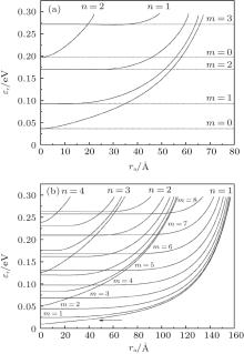
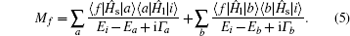
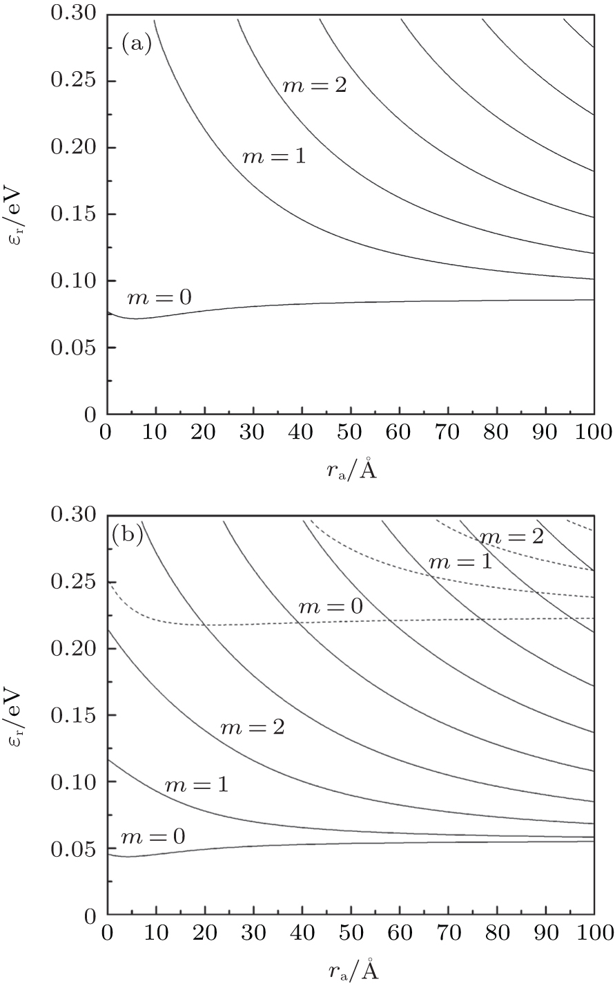
Consider first the behaviors of the electronic states for a semiconductor quantum well/shell of cylindrical geometry formed in a matrix of GaAs/Al0.35Ga0.65As, the parameters needed are μ 1 = 0.0665μ 0, μ 2 = 0.096μ 0, and V0 = 0.30 eV, [43] where μ 0 is the free electron mass. Figure 1(a) shows the energies corresponding to the system with rb = 100 Å . The straight lines represent the energies of a quantum wire with a radius of 100 Å , obtained using Eq. (2). It can be seen that increasing ra causes an increase in energy for all the different states of the QWW due to the fact that we increase the confinement of the electrons. It is also visible that these increases in energy are not the same for all levels. The increase of ra means the increase of the confinement, and it can remove all levels within the QWW. This effect is modulated by the barrier height of the system. From Figs. 1(a) and 1(b), it can be concluded that the states are grouped into several sub-bands; these sub-bands are determined by the quantum number n. When n is larger, the energies of the states that make up the sub-band are bigger. Within each sub-band, there are levels with quantum number m, and the energy increases with increasing m. As can be seen in Fig. 1(a), the energy of the state with m = 0 and n = 1 is almost constant up to ra = 4 Å , the remaining values are similar to those of a quantum wire with ra = 0 Å and rb = 100 Å ; while the energy of the state with m = 1 and n = 1 is almost constant up to ra = 15 Å , and the energy of the state with m = 2 and n = 1 is almost constant up to ra = 25 Å . This means that the effect of the confinement on the quantum state decreases with increasing energy and quantum number m in each sub-band (see Fig. 1(b)). In Fig. 1(b), we increase the radius to rb = 200 Å . As shown in this figure, this increase causes the states to significantly reduce their energy, with a greater reduction for states with higher quantum numbers m and n. Also, in this case, it is seen that increasing rb involves increasing the number of states “ within” the system. Furthermore, crosses are observed between the levels of different sub-bands, but not between levels of the same sub-band.
 | Fig. 1. Electron energies ε r corresponding to a semiconductor quantum well wire with (a) rb = 100 Å , (b) rb = 200 Å . The dotted line in panel (a) corresponds to the energy of a quantum well wire with ra = 0 Å and rb = 100 Å . |
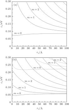
In Fig. 2, we study QWW of various widths (a) d = 80 Å , (b) d = 100 Å ; where the solid and dashed lines correspond to the states with n = 1 and n = 2, respectively. As can be observed, the states are grouped into sub-bands, again determined by the quantum number n. It can be observed that increasing the width increases the number of energy levels within the QWW. Moreover, increasing ra leads to more energy levels in the well because the QWW system volume increases. In the case that ra is approximately 300 Å , it does not reproduce the energy values corresponding to a quantum well of width d because even for these radii, the cylindrical symmetry is preserved. Furthermore, it is interesting to note that the states tend to minimal energy for each n. This is due to the fact that QWW always has a fixed width, so for ra → ∞ it should reproduce the energy values corresponding to a quantum well with width d.[43]
Equations (10) and (11) have resonant singularities which are independent of the incident photon or the secondary photon when

and non-resonant singularities which are dependent on the incident photon or the secondary photon when


where a = 2 for 


 | Fig. 2. The electron energies ε r corresponding to a semiconductor quantum well wire with (a) d = 80 Å , (b) d = 100 Å . The solid line corresponds to n = 1 electron states, and the dotted line corresponds to n = 2 electron states. |
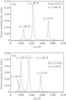
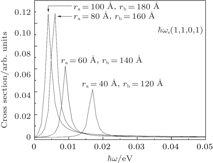
In general, the system behavior is very similar to that described in Ref. [42], considering that B = 0 T; however, some differences are detailed below. Figure 3(a) shows the differential cross section for the polarizations 
 | Fig. 3. Differential cross section for a semiconductor quantum well wire with  |
 | Fig. 4. Differential cross sections for a semiconductor quantum well wire with |
We present the formulas for calculating the electron Raman scattering intensities for the semiconductor quantum well wire with a cylindrical ring cross-section grown in a GaAs/Al0.35Ga0.65As matrix. Furthermore, we demonstrate that the structure of the differential cross-section as given in figures, provides a transparent understanding of the energy sub-band structure. The results presented in this work are similar to those previously obtained in other theoretical work.[42] Moreover, we show that any change in the system configuration leads to changes in the intensity and the frequency of the secondary radiation. This effectively shows that Raman spectroscopy is a powerful probe for semiconductor nanostructures due to the material-selective resonant enhancement. In addition, we note that in this work we have applied a simplified model for the electron structure of the system. In a more realistic case, we should consider a coupled band structure by using models like the Luttinger– Kohn or the Kane model. The Raman scattering process considering the electron– phonon interaction is studied using the dielectric continuum approach which has separate sets of confined and surface (interface) modes.
| 1 |
|
| 2 |
|
| 3 |
|
| 4 |
|
| 5 |
|
| 6 |
|
| 7 |
|
| 8 |
|
| 9 |
|
| 10 |
|
| 11 |
|
| 12 |
|
| 13 |
|
| 14 |
|
| 15 |
|
| 16 |
|
| 17 |
|
| 18 |
|
| 19 |
|
| 20 |
|
| 21 |
|
| 22 |
|
| 23 |
|
| 24 |
|
| 25 |
|
| 26 |
|
| 27 |
|
| 28 |
|
| 29 |
|
| 30 |
|
| 31 |
|
| 32 |
|
| 33 |
|
| 34 |
|
| 35 |
|
| 36 |
|
| 37 |
|
| 38 |
|
| 39 |
|
| 40 |
|
| 41 |
|
| 42 |
|
| 43 |
|
| 44 |
|