Liu Can-Huaa), b)  , Jia Jin-Feng
a), b)
, Jia Jin-Feng 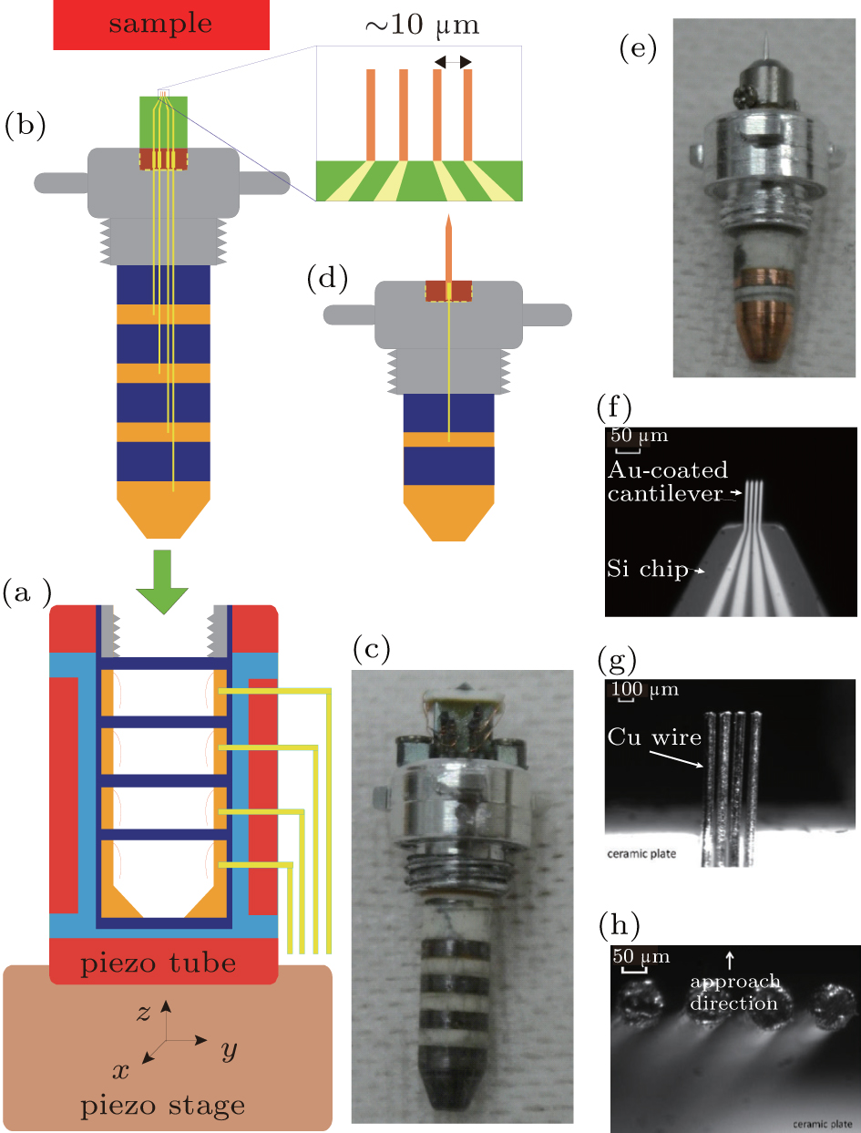
|
Liu Can-Hua
, Jia Jin-Feng |
| Development of 4PP that is compatible with STM.[ 40 ] (a) Schematic drawing of the deformed probe stage. (b), (c) Schematic drawing and photograph of the 4PP holder, respectively. (d), (e) Schematic drawing and photograph of the STM tip holder, respectively. (f) Photograph of Si-chip based micro-4PP, taken via optical microscope. (g), (h) Photograph of Cu-wire 4PP taken from different view angles via optical microscope. |
| |