Liu Can-Huaa), b)  , Jia Jin-Feng
a), b)
, Jia Jin-Feng 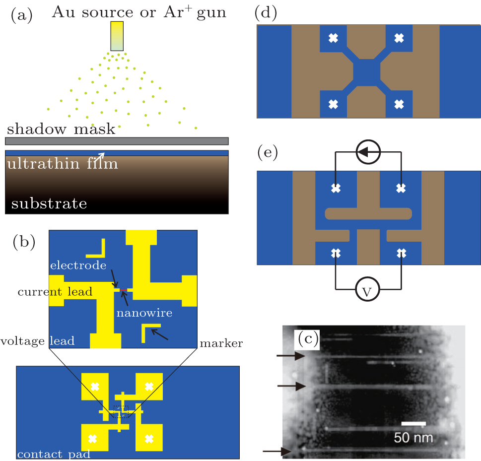
|
Liu Can-Hua
, Jia Jin-Feng |
| (a) Schematic illustration of a nanostenciling setup. Yellow spots represent Au atoms (Ar+ ions) evaporated (sputtered) from a Au source (Ar+ gun). (b) Schematic drawing of electrode patterning fabricated by nanostenciling. It is used for in situ two-terminal transport measurement of nanowires. Upper: close up around the center; lower: overview. (c) STM image of two electrodes connected with ErSi2 nanowires. The arrows indicate the nanowires bridging the electrode gap.[ 23 ] (d), (e) Schematic drawing of sample patterning in Van der Pauw’s and linear configurations, respectively, for in situ four-terminal transport measurement of superconductive ultrathin films. Blue areas are the -In surface, and grey are Si(111) surface sputtered by Ar+ ions. |
| |