
GaInP/GaAs tandem solar cells with highly Te- and Mg-doped GaAs tunnel junctions grown by MBE
[Zheng Xin-He†a), b)  , Liu San-Jie
a) , Xia Yua) , Gan Xing-Yuanb) , Wang Hai-Xiaob) , Wang Nai-Mingb) , Yang Huib) ]
, Liu San-Jie|
|

 , Liu San-Jie
†Corresponding author. E-mail: xinhezheng@ustb.edu.cn, or xhzheng2009@sinano.ac.cn
*Project supported by the SINANO-SONY Joint Program (Grant No. Y1AAQ11001), the National Natural Science Foundation of China (Grant No. 61274134), the USCB Start-up Program (Grant No. 06105033), and the International Cooperation Projects of Suzhou City, China (Grant No. SH201215).
We report a GaInP/GaAs tandem solar cell with a novel GaAs tunnel junction (TJ) with using tellurium (Te) and magnesium (Mg) as n- and p-type dopants via dual-filament low temperature effusion cells grown by molecular beam epitaxy (MBE) at low temperature. The test Te/Mg-doped GaAs TJ shows a peak current density of 21 A/cm2. The tandem solar cell by the Te/Mg TJ shows a short-circuit current density of 12 mA/cm2, but a low open-circuit voltage range of 1.4 V∼1.71 V under AM1.5 illumination. The secondary ion mass spectroscopy (SIMS) analysis reveals that the Te doping is unexpectedly high and its doping profile extends to the Mg doping region, thus possibly resulting in a less abrupt junction with no tunneling carriers effectively. Furthermore, the tunneling interface shifts from the intended GaAs n++/p++ junction to the AlGaInP/GaAs junction with a higher bandgap AlGaInP tunneling layers, thereby reducing the tunneling peak. The Te concentration of ∼ 2.5 × 10²⁰ in GaAs could cause a lattice strain of 10−3 in magnitude and thus a surface roughening, which also negatively influences the subsequent growth of the top subcell and the GaAs contacting layers. The doping features of Te and Mg are discussed to understand the photovoltaic response of the studied tandem cell.
Conventional III– V compound semiconductor multi-junction solar cells have developed into an important means of power generation in terrestrial and space applications. Very recently, a world-record 44.7% photovoltaic (PV) conversion efficiency using a new cell structure with four subcells at a concentration of 297 suns was achieved.[1] Also, Spectrolab Inc. reports a wafer-bonded five-junction space cell with an efficiency of 35.1% for AM0 1 sun.[2] One critical part in these multi-junction solar cells is the use of tunnel junctions (TJ) that electrically interconnect the subcells.[3] For a good tunnel junction, high doping levels and abrupt doping profiles are required on both sides of the junction. Molecular beam epitaxy (MBE) systems may use solid-state sources for group V materials, thus avoiding the use of hazardous gases such as PH3 and AsH3, which are widely utilized in metal-organic vapor phase epitaxy (MOVPE). Therefore, the MBE technique has always been a very interesting and ecologically clean tool for the growth of III– V tandem solar cells.[4– 9] Recently, a significant contribution from MBE to the field of III– V tandem solar cells has been the rapid progress of MBE-grown GaInNAs(Sb) alloys as 1-eV materials, [10] and the subsequent world efficiency record was held for some time.[11] Additionally, one key advantage of MBE technique today is that a wide range of high quality materials that can be implemented in tandem cells.
In the MBE method, Si and Be are frequently used as dopants in GaAs tunnel junctions to electrically interconnect GaInP/GaAs tandem solar cells. Due to the amphoteric dopant nature of Si, [12, 13] Si-doped GaAs encounters a significant self-compensation problem when the dopant concentration is above 5 × 1018 cm− 3. In addition, Be strongly diffuses in GaAs and is highly toxic.[14– 16] To overcome these disadvantages, researchers have proposed Te as an n-type dopant for GaAs and Mg as a p-type dopant, [13, 17– 20] since GaAs can be heavily doped with Te and Mg and they have very low diffusion coefficients, which is beneficial to the production of abrupt doping profiles in GaAs tunnel junctions. Recently, it has been reported that GaInP/GaAs tandem cells were used as a GaAs tunnel junction with Te doping in n+ + -GaAs via MOVPE.[13] To date, a combination of Te and Mg dopants used in GaAs devices has not been reported. In our previous study, via an optimization of heavily Te- and Mg-doped GaAs growth by MBE, a peak current density of 21 A/cm2 for the Te/Mg tunnel junction was demonstrated. The detailed growth and tunneling properties of the tunneling junction have been reported elsewhere.[21]
In the present work, the photovoltaic response of GaInP/GaAs tandem solar cells using the Te/Mg tunnel junction is investigated in detail. The GaInP/GaAs tandem solar cells which are interconnected by this TJ show a high short-circuit current density of over 12 mA/cm2 but have a comparatively low open-circuit voltage (Voc). The reason behind this performance is discussed in this paper.
The samples studied in this work were grown on GaAs (001) substrates by a Veeco GEN20A dual chamber solid-state MBE system equipped with reflection high-energy electron diffraction (RHEED) apparatus that was used to monitor the growth rate and surface morphology of the epilayers. One chamber is for heavily doped GaAs, with tellurium (Te) and magnesium (Mg) elemental sources serving as normal dual-filament low temperature effusion cells. The growth conditions (including growth temperature and source temperature/beam equivalent pressure) were optimized to obtain the carrier densities required for Te and Mg doping in the GaAs layers. The other chamber is for the growth of GaInP (1.88 eV)/GaAs solar cells and the GaInP barrier layer of the GaAs tunnel junction on p-GaAs substrate. Additionally, single-junction GaInP devices with the same band-gap as the top GaInP subcell in the GaInP/GaAs dual-junction solar cells with the Te/Mg TJ were grown and fabricated. We first fabricated and tested GaAs/GaAs tunnel junctions with GaInP barriers by using Te as the n-type dopant and Mg as the p-type dopants (denoted as the Te/Mg tunnel junction). The heavily doped GaAs layers in the Te/Mg tunnel junction are designed to have electron and hole concentrations of 1.5 × 10¹⁹/cm3 and 1 × 10¹⁹/cm3, respectively. For the heavy Te and Mg doping, due to their volatilities, we employed a low growth temperature in the growth region of the tunnel junction. Through many optimizations of growth conditions such as growth temperature, Te source temperature, Mg source temperature, etc., the heavily doped n-type and p-type GaAs samples produced a high carrier density of 1 × 10¹⁹/cm3– 2 × 10¹⁹/cm3 with a still reasonably-high mobility. According to the designed carrier densities in the GaAs/GaAs tunnel junction, we utilized a growth temperature of 470 ° C (from pyrometer calibration) for the n+ + -GaAs(Te) layer and 370 ° C (from thermal couple setting) for the p+ + -GaAs(Mg) layer. For the Te/Mg tunnel junctions, a typical 4-probe time-averaged measurement of the I– V behavior of the mesa structure with a dimension of 0.1 cm × 0.1 cm was used. Measurements were performed under dark and temperature-controlled conditions (25.0 ° C). The fabricated GaInP/GaAs tandem solar cells, which have the device parameters schematically shown in Table 1, have an area of 0.22 cm2. Standard photolithography techniques were used to process both the tunnel junctions and the solar cells.
| Table 1. Schematic structure parameters of dual-junction solar cell with the GaInP/GaAs subcells connected by the Te/Mg tunnel junctions. |
The p-GaAs and n-GaAs Ohmic contacts were based on Pd/Zn/Pd/Au and AuGe/Ni/Au metal systems, respectively. Forming gas (4% H2/95% N2) annealing was carried out at 340 ° C for 10 min to form the n-type Ohmic contact while the p-type Ohmic contact was processed at 420 ° C for 30 s in an N2 atmosphere. The shadow loss of the front contacts is around 5%. A triple layer SiOx/TiOx/SiOx antireflective coating (ARC) was finally deposited on the device, which was then encapsulated. The devices were characterized using a microprobe station under an AM1.5G solar simulator from Abet Technologies’ Sun 2000 family of solar simulators. A current– voltage (I– V) curve was recorded by a Keithley 2440 source meter. Before measurements, a standard silicon detector was used to calibrate the AM1.5 solar spectra, which is defined as one sun of AM1.5 with a spectral mismatch factor of 0.92. The I– V data were corrected by the spectral mismatch factor. The devices were placed on a heat sink with a closed water circuit to optimize the thermal management. A 4-probe design using soldered bonding wires was employed to make contact with the cells. All of the measurements were recorded at 25.0 ° C monitored by using a thermocouple mounted adjacent to the solar cell.
The test of the Te/Mg tunnel junctions employs GaInP and AlGaInP barrier layers. Based on the doping optimization in MBE experiments, the heavily Mg-doped p+ + -GaAs layer in the TJ is designed to have a thickness of 15 nm and a carrier concentration of 1 × 10¹⁹/cm3 which has a mobility of 40 cm2/V· s. The 12-nm-thick n+ + -GaAs: Mg layer has a hole densities of 2 × 10¹⁹/cm3, corresponding to 650 cm2/V· s in mobility. Figure 1 shows the typical current– voltage characteristic curve of the Te- and Mg-doped GaAs tunnel junctions. A peak current density of 21 A/cm2 is observed in the bias regime of around 100 mV.[21] At present, high performance tandem GaInP/GaAs or GaInP/InGaAs/Ge solar cells have a short-circuit current density of around 15 mA/cm2 at one sun.[22– 24] If the voltage drop of the tunnel junction within multiple junction solar cells is not significantly increased under concentration conditions, the tunnel junction could afford a current interconnection of all subcells till 1000 suns. However, the peak-to-valley ratio is not so high (or large valley current), indicating that the excess current is significant. This could be ascribed to microdefects, clusters, stacking faults, and nonreactive species in highly doped GaAs tunnel junction layers. Such defects could create levels in the band gap, causing significant excess current through trap-assisted tunneling.[13] Actually, excess current in a good tunnel junction is not particularly important because it will not affect the device performance even under concentration.
 | Fig. 1. Typical I– V characteristic curve of the heavily Te- and Mg-doped GaAs/GaAs TJ’ . |
A differential resistance calculation provides evidence that the tunneling region corresponds to a total series resistance of 10− 3 Ω · cm2. Therefore, in terms of the operation in concentration conditions and practical voltage drop (< 15 mV), such tunnel junctions would be suitable for high efficiency devices under 200X– 400X suns. In Ref. [25], the authors reported a very low resistance of 1.6 × 10− 5 Ω · cm2 for an AlGaAs:C/GaAs:Te tunnel junction grown by MOVPE. The GaInP/GaAs solar cells in our study, connected in series by the Te/Mg tunnel junction, might be negatively influenced by its comparatively large resistance.
In addition, it is worth pointing out that a wide Te distribution in this test tunnel junction is observed, which leads to the pn junction of the tunneling junction where [Mg] is much larger than [Te] shifting closer to the interface between GaAs:Mg and AlGaInP barrier layers. Therefore, tunneling still occurs readily, resulting in a high peak current density. Meanwhile, a forward diffusion of Te into the AlGaInP barrier layers will influence the subsequent epilayer growth of the GaInP/GaAs tandem solar cell using the electrically interconnected Te/Mg tunnel junction. To alleviate this diffusion due to the strong memory effect of Te and/or Mg, the MBE system is baked again prior to the epilayer growth of GaInP/GaAs tandem cells.
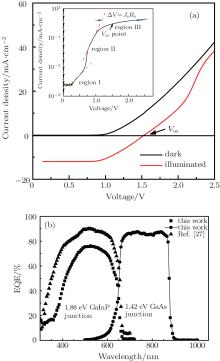
Figure 2(a) shows a normal shape of the light I– V curves of the GaInP/GaAs tandem solar cells, which are electrically interconnected in series by the Te/Mg tunnel junction under one sun illumination. The devices display a short-circuit current density (Jsc) of over 12 mA/cm2 and an open-circuit voltage (Voc) of 1.53 V. It is seen that the devices have a reasonably high Jsc as compared with that of the reported GaInP/GaAs tandem solar cells.[26]
 | Fig. 2. (a) Typical J– V curves of GaInP/GaAs tandem solar cells under dark and illuminated conditions. The inset shows a dark J– V curve on a semi-logarithmic plot in which different regions are indicated, (b) EQE (solid square and circle) for the same devices. The solid triangle shows the EQE of the single GaInP solar cell reported in Ref. [27]. |
The values of Jsc calculated by means of the convolution of the EQE values as shown in Fig. 2(b), obtained for ARC-coated devices with the standard solar spectrum AM1.5G, are 12.1 mA/cm2 and 13.0 mA/cm2 for the top GaInP and bottom GaAs cells, respectively. The current mismatch is estimated to be 6.9%. This means that there is still room to improve the tandem devices with the Te/Mg tunnel junctions. It is interesting to note that the calculated Jsc value of the bottom cell is close to that of the reported GaInP/GaAs tandem solar cells.[22] This result implies that the GaAs bottom cell after the growth of a Te/Mg tunnel junction is still good for the extraction of photon-generated carriers. In addition, the EQE clearly reveals a maximum value of around 75%, which is much lower than the reported value.[22, 26, 27] Actually, the reported GaInP single-junction solar cells with using the same MBE chamber have been observed to show a good photovoltaic performance with an open-circuit voltage of over 1.37 V, a short-circuit current density of 13.5 mA/cm2 and a maximum EQE value of around 89%[27] as shown in Fig.2(b). Therefore, these limitations to the collection of photo-generated carriers for the top subcell in a wavelength range of 300 nm– 650 nm show that no good performance GaInP subcells is achieved after the growth of Te/Mg tunnel junctions.
Actually, in our experiments, an efficient ARC is optimized in the entire spectral range for the single-junction and dual-junction solar cells. The reflectivity dependences on wavelength are very similar for all solar cells fabricated. Therefore, a lower EQE and Jsc of the top cell could be ascribed to the influence of the Te/Mg tunnel junction on the subsequent growth of the top subcell layer in the real structure. In terms of the EQE reduction within the entire wavelength range in which the cell responses, the lower EQE of the GaInP subcell should be attributed to a decrease of internal quantum efficiency, which is caused by high interface recombination and a shorter Shockley– Read– Hall lifetime in the active region. In particular, the later culprit could result from poorer crystalline quality of the top subcell. This is discussed below, based on the SIMS and structural analysis of the samples.
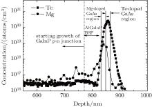
However, the low Voc and FF for the tandem devices are beyond our expectations. According to the electrical properties of the Te/Mg tunnel junction and a possible influence on the subsequent growth of the top cell and GaAs contacts, we will continue to discuss the growth behavior of the Te/Mg tunnel junction. Figure 3 shows SIMS profiles of the Te and Mg after the growth of the entire device structure.
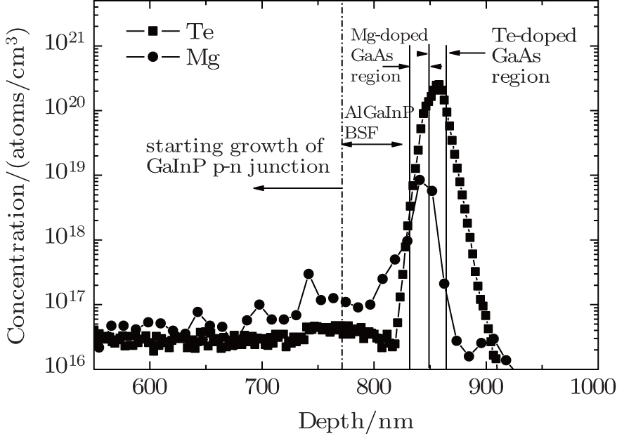 | Fig. 3. SIMS profiles of Te and Mg elements in the tunnel junctions and the top GaInP subcells. |
There are no significant diffusions of Te and Mg dopants into the subsequent GaInP top subcell. However, the Te concentration in the tunnel junction reaches 2.5 × 10²⁰/cm3, which is much higher than the designed doping value. Based on our previous report, [21] a Te incorporation concentration of around 3 × 10¹⁹/cm3 into GaAs can produce an electron density of 1.5 × 10¹⁹/cm3. Furthermore, it is worth noting that while the Te incorporation density is over 5 × 10¹⁹/cm3, the electron concentration reduces to (3∼ 4) × 1018/cm3. It is also found that the samples look misty on the surface, which could be induced by an introduction of defects. Therefore, these results provide evidence that the surplus Te and induced defects will start to compensate for the Te-doped GaAs, thus leading to a significant reduction of electron concentration after a maximum value has been reached. This unexpected incorporation ratio of Te elements could be ascribed to a strong memory effect due to the use of a normal effusion cell. In addition, the SIMS profile indicates a broadening of the carrier concentration distribution for Te donors in GaAs, which is almost an order of magnitude larger than the Mg concentration in the p-type GaAs material. The Te distribution results in a shifting of the interface where [Mg] > [Te] closer to the AlGaInP BSF. The tunneling interface shifts from the intended GaAs n+ + /p+ + junction to the AlGaInP/GaAs junction with a higher bandgap of AlGaInP as compared with the GaAs tunneling layers, reducing the tunneling peak[28] and thus resulting in a strong decrease in Voc. Furthermore, due to the limited Mg in p-type region of the tunnel junction, the net p-type doping concentration is also sharply reduced. Therefore, this would most likely result in a lower hole concentration in the p-GaAs layer, causing the tunnel junction not to tunnel the carriers effectively and finally reducing the peak current density and increasing the series resistance, which are reflected by J– V curves, as shown in Fig. 2(a). Additionally, it could be interesting to point out that a close view of SIMS profile reveals a non-negligible forward diffusion of Te into the AlGaInP BSF layers. The interface quality could have a negative influence on the Voc by introducing a strong concentration of interface traps. This could also reduce the Voc of the GaInP top subcell.
The effect of the series resistance can be analyzed from a plot of the current– voltage characteristic at a larger applied voltage, which is required to achieve the same current value when a series resistance is included.[28] Figure 2(a) shows typical J– V characteristics of the solar cells in the dark conditions. From a J– V curve on a semilog scale, shown in the inset of Fig. 2(a), three regions are divided. At small voltage less than 0.6 V, recombination current predominates. A different ideality factor from that of region I is seen from the straight-line relationship between current density and applied voltage, indicating that the diffusion current predominates while the voltage ranges from 0.7 V to 1.1 V. For the applied voltages beyond Voc point, the line significantly deviates from linearity, which shows that the region is dominated by a large series resistance. Note that the Te/Mg TJ works under reverse bias. Under reverse bias, in terms of classical tunnel junction theory, tunnel junction current densities typically increase without limit due to the increasing overlap of filled states in the p-type region with empty states in the n-type region. By using a voltage drop from the series resistance (Δ V = JsRs), approximately 44 Ω · cm2 of series resistance is extrapolated. The series resistance is much larger than a sum (around 4.4 Ω · cm2 for the same device size) of the resistance of single-junction GaInP solar cells and that of single-junction GaAs solar cells. The results indicate that the tunnel junction limits the cells. Furthermore, this limitation is reflected by the behavior of the illuminated J– V characteristics of the tandem cell at voltages larger than Voc where the Te/Mg TJ works as a reverse diode. It can be seen that when the applied voltage increases from 1.6 V to 2.1 V, the illuminated J– V curves show a similar tendency to those of the dark conditions for the voltages ranging from 0.7 V to 1.1 V in which a mediate current is injected. However, note that the series resistance dominates the J– V characteristics at high currents while the voltage is above 2.1 V. The results show that the tunnel junction has not completed a good tunneling effect, thus leading to a large resistance. The large resistance induces not only the low FF (∼ 55%), but also a high voltage drop at the tunnel junction under operating conditions, thus resulting in a lower Voc of the cells.
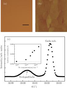
To further verify a possible influence from Te- and/or Mg-doping, we perform ex situ characterization of GaAs layers with the same concentration as that of the designed GaAs tunnel junction with using Te and Mg dopings. Figures 4(a) and 4(b) show optical microscope and atomic force microscope images, respectively, for the Mg-doped p+ + -GaAs sample with a carrier concentration of 1 × 10¹⁹/cm3. The samples display a mirror-like and atomically-resolved smooth surface (0.3-nm room-mean-square roughness), which should be good enough to support the subsequent growth. x-ray diffraction analysis also reveals no peak separation from the peak out of the substrate (not shown here). That is, the lattice of the Mg-doped GaAs is completely matched to that of the GaAs substrate. However, it is important to note that, as shown in Fig. 4(c), there is a peak separation for the heavily Te-doped n+ + -GaAs layers with a carrier density of 1.5 × 10¹⁹/cm3. This separation arises from a compressive strain with a lattice mismatch of 6 × 10− 4, which leads to a lattice constant of 5.6568 Å (5.6534 Å for a GaAs substrate). Note that the x-ray diffraction is measured using a test thicker sample with a carrier density of 1.5 × 10¹⁹/cm3 as obtained by the Hall effect. For this sample, the Te-doping concentration is around 3 × 10¹⁹/cm3 obtained by SIMS analysis. However, as shown in Fig. 3, due to a Te memory effect, an unexpected doping concentration of 2.5 × 10²⁰/cm3 is observed in the Te-doped GaAs region during the growth of the solar cells, which will induce a lattice mismatch and/or compressive strain. The lattice constants are measured by a developed method[29] from the Bragg’ s law, as a function of Te concentration, shown in the inset of Fig. 4(c). It is found that a mismatch of 1.6 × 10− 3 is induced while a Te-doping concentration reaches 2.3 × 10²⁰/cm3 which is close to the concentration of Te incorporation into GaAs in the current TJ’ s. In terms of a dependence of the critical thickness on a given misfit in the case of zincblende crystals, the mismatch of 1.6 × 10− 3 could afford a coherent strain layer with a thickness of 100 nm– 150 nm on GaAs, without introducing misfit dislocations.[30] Now, the Te-doped GaAs tunneling region is below the critical thickness. Therefore, the probability of the formation of threading dislocations in the Te-doped GaAs and the subsequent GaInP cell layers should be extremely low. Based on the epi-growth theory, [30, 31] due to unexpectedly high Te-doping concentration of 2.5 × 10²⁰/cm3, the compressive strain will lead to a surface undulation (or rough surface) of the thin Te-doped n+ + -GaAs tunnel junction layer which could degrade the crystalline quality of the subsequent growth of Mg-doped p+ + -GaAs and the GaInP top cell. As earlier reported, after the growth of Te- and Mg-doped GaAs TJ’ s at low growth temperature, a thermal treatment at 580 ° C for 5 min is introduced to improve the surface morphology. However, a completely smooth one, characterized by RHEED patterns, is not achieved, which is probably due to double negative influence on the epi-growth. This negative influence is also reflected by an observation of not-so-streaky RHEED patterns during the subsequent growth of GaInP subcell layers. In addition, it should be noted that, due to the Te memory effect, the as-grown sample has a misty surface morphology. This phenomenon could degrade the surface quality of device, increasing contact resistance and possibly damaging the GaInP epilayers. Therefore, inadequate crystalline quality of the top GaInP subcell could finally result in a reduction of tandem Voc and a limited Jsc. Also, it is worth noticing that the induced strain will have a negative effect on the surface of the GaAs contacting layers, which will introduce a large series resistance into the cell.
 | Fig. 4. (a) Optical (200X) and (b) atomic force microscopy images (scanning area: 1 μ m × 1 μ m) of Mg-doped GaAs layers on a GaAs substrate, (c) x-ray diffraction profile of Te-doped GaAs layer. The inset shows the lattice constants of the Te-doped samples as a function of Te concentration measured by SIMS. The lattice constant of GaAs substrate is indicated as a dot line. |
We report preliminary results on GaInP/GaAs tandem solar cells which are electrically interconnected via Te/Mg tunnel junctions grown via MBE. A reasonably-high Jsc of over 12 mA/cm2 is achieved for the cell devices fabricated. A memory effect of Te due to the use of a normal effusion cell may be responsible for a sharp increase in Te incorporation and could widen its distribution in the tunnel junction, and even into the AlGaInP BSF of the GaInP top subcell. Owing to a too heavy doping concentration, the large compressive strain in the n+ + -GaAs layer may lead to strain-induced roughening of a thin epitaxial film which negatively influences the subsequent growing of the top cell layers and the GaAs contacting layers. A low Voc of the tandem cells interconnected by the Te/Mg tunnel junction should be ascribed to the tunnel junction, which is reflected by the lower carrier concentration in p-type doping region and higher series resistance reflected by the J– V characteristics of the tandem cell at voltages larger than Voc, as well as inadequate crystalline quality reflected by the lower EQE as compared with the GaInP single-junction cell. This could potentially be alleviated through an insert added to the bottom of the crucible or the use of a cracking furnace.
We are grateful to Dr. Tamzin Lafford, ESRF, for reading the manuscript. And we specially thank M. Ikeda, S. Uchida, and M. Arimochis, from Sony Corporation, Japan for SIMS measurements and device processing.
| 1 |
|
| 2 |
|
| 3 |
|
| 4 |
|
| 5 |
|
| 6 |
|
| 7 |
|
| 8 |
|
| 9 |
|
| 10 |
|
| 11 |
|
| 12 |
|
| 13 |
|
| 14 |
|
| 15 |
|
| 16 |
|
| 17 |
|
| 18 |
|
| 19 |
|
| 20 |
|
| 21 |
|
| 22 |
|
| 23 |
|
| 24 |
|
| 25 |
|
| 26 |
|
| 27 |
|
| 28 |
|
| 29 |
|
| 30 |
|
| 31 |
|