


A threshold voltage model of short-channel fully-depleted recessed-source/drain (Re-S/D) SOI MOSFETs with high- k dielectric
[Krishna Saramekala Gopia) , Dubey Sarveshb) , Kumar Tiwari Pramod†a)  ]
]
]
|
|


†Corresponding author. E-mail: tiwarip@nitrkl.ac.in
*The author, Pramod Kumar Tiwari, was supported by the Science and Engineering Research Board (SERB), Department of Science and Technology, Ministry of Human Resource and Development, Government of India under Young Scientist Research (Grant No. SB/FTP/ETA-415/2012).
In this paper, a surface potential based threshold voltage model of fully-depleted (FD) recessed-source/drain (Re-S/D) silicon-on-insulator (SOI) metal-oxide semiconductor field-effect transistor (MOSFET) is presented while considering the effects of high- k gate-dielectric material induced fringing-field. The two-dimensional (2D) Poisson’s equation is solved in a channel region in order to obtain the surface potential under the assumption of the parabolic potential profile in the transverse direction of the channel with appropriate boundary conditions. The accuracy of the model is verified by comparing the model’s results with the 2D simulation results from ATLAS over a wide range of channel lengths and other parameters, including the dielectric constant of gate-dielectric material.
Over the past few years, considerable attention has been paid to recessed-source/drain (Re-S/D) silicon-on-insulator (SOI) metal-oxide semiconductor field-effect transistor (MOSFET) by both academic researchers and the semiconductor industry due to its better drive current capability than that of the conventional SOI MOSFET.[1– 9] In the recessed-source/drain SOI MOSFET, source and drain are extended deeper into the buried oxide (BOX) in order to mitigate the effects of large source and drain resistances, which originate from the ultrathin body structure.[10, 11] A number of analytical models have already been presented for short-channel Re-S/D SOI MOSFETs to address various subthreshold parameters, such as threshold voltage, [3– 5] subthreshold current, and subthreshold swing.[6, 7]
As SOI MOSFET has a highly scalable structure. An ultrathin gate oxide (tox < 2 nm), which is of the SiO 2 in general, is needed to curb the short-channel effects if the device channel length goes below 32 nm.[12] However, an ultrathin gate oxide of thickness less than 2 nm causes a higher leakage current density, which arises mainly from the quantum-mechanical direct tunneling through the gate oxide.[13] Therefore, suitable high-k gate-dielectrics with good physical property and low electrical thickness have been looked for in order to control both short-channel effects and gate leakage current simultaneously. HfO2 (relative permittivity ε k = 22), ZrO2 (ε k = 25), and Ta2O5 (ε k = 26) are found to possess excellent performance with high permittivity and energy gap.[14, 15] High on-current and reduced subthreshold swing have already been reported for SOI double-gate MOSFETs by carefully choosing the gate-dielectric material.[16] However, the use of a thicker high-k dielectric material in place of SiO2 causes considerable fringing-field lines, which in turn modulate the source-channel barrier height, resulting in the change of subthreshold characteristics.[17– 24] The effect of fringing-field lines on the subthreshold characteristics of SOI MOSFET is modeled in terms of a fringing capacitance Cbot.[20] The fringing capacitance is attributed to the electric field interaction between the bottom of gate electrode and source/drain region through the side-wall spacer, as shown in Fig. 1. A large number of theoretical models of Cbot have been presented in the technical literature[20– 24] for different complementary metal-oxide semiconductor (CMOS) devices. Mohapatra et al.[23] developed a parasitic capacitance model in deep submicrometer conventional high-k dielectric metal-oxide semiconductor (MOS) transistor in the presence of source/drain electrodes by considering three types of parasitic capacitances: Cside, the sidewall fringing capacitance between gate and source/drain regions (through high-k); Cpp, the parallel plate capacitance between gate and source/drain electrodes; Ctop the top fringing capacitance between top surface of the gate and source/drain electrodes through the first layer of passivation dielectrics. Later, Kumar et al.[20] developed a parasitic capacitance model for high-k gate-dielectric silicon-on-insulator (SOI) MOSFET by considering the effect of the parasitic internal fringe capacitance associated with the bottom edge of the gate electrode and the source and drain regions. They also developed a threshold voltage model for SOI MOSFET including the fringing capacitance model.[20] A compact model of fringing field induced parasitic capacitance for MOSFET has been developed by Liu et al.[24] They have used conformal mapping method to derive the capacitance Cbot.[24]
 | Fig. 1. Schematic structure of the Re-S/D FD SOI MOSFET, showing the internal parasitic fringe capacitance. |
However, the effect of high-k dielectric on the subthreshold characteristics of Re-S/D SOI MOSFETs has not been analyzed to date, either experimentally or analytically. In this paper, we present a threshold voltage model, which is an important subthreshold characteristic, of Re-S/D SOI MOSFET with high-k dielectric by considering the influence of fringing field in terms of capacitance Cbot. The two dimensional (2D) Poisson’ s equation is solved in a channel region in order to determine the electrostatic potential. Furthermore, the surface potential, which is obtained from 2D electrostatic potential, is modified by adding a potential V(x) in order to capture the effect of high-k dielectric induced fringing field. Moreover, to invoke the effect of lightly doped substrate, which is used generally in practice, a substrate induced surface potential (SISP) parameter is also introduced in the boundary conditions.[25] Subsequently, the minimum of surface potential is utilized to present the threshold voltage model. Both amorphous and epitaxial silicon are found to be used for extended source/drain in Re-S/D SOI MOSFET.[26– 29] Thean et al.[26] etched out portions of both channel and BOX by selectively using HF solution and they subsequently deposited epitaxial silicon as source and drain regions, including the extended regions in the BOX. On the other hand, Bin[27] in his patent reported that amorphous semiconductor layer is used to form recessed source/drain. The model results are verified by comparing them with the simulated results which are obtained from the 2D simulator from SILVACO.[30]
The schematic structure of the Re-S/D UTB SOI MOSFET device with high-k gate-material used in our analysis and simulation is shown in Fig. 1. Here, L, w, tSi, tgt, tsp, tox, and tbox are the gate length, channel width, channel thickness, thickness of gate, length of spacer, gate-dielectric thickness, and the thickness of BOX, respectively; trsd and dbox are the source/drain penetration in the BOX and the length of source/drain overlap over the BOX, respectively. A doping concentration Na is assumed to be uniform in the silicon channel region. The high-k gate-dielectric considered for modeling and simulations is HfO2 with a permittivity (ε k) of 22, unless otherwise stated. The entire channel region is considered to be ultrathin to avoid the consequence of floating body effects. The x and y axes are considered to be along the channel length and channel thickness respectively as shown in the schematic structure. The drift-diffusion (DD) model of carrier transportation is taken into account in device simulation. The CVT mobility model is also used as it is a versatile mobility model in which mobility depends on many parameters such as doping density, temperature, parallel electric field and vertical electric field. ATLAS default model parameter β and vsat.n are modified by setting β = 1 and vsat.n = [(1.5L + 21.6)/(L + 2.7)] × 107 cm/s (where L is in nm).[31] This modification is performed in order to calibrate the model results with simulation results as the default DD model of ATLAS simulator starts to predict the inaccurate results in sub 100-nm channel length regime and, therefore, some modifications to the parameters are required. The Fermi– Dirac carrier statistical model is employed to minimize carrier concentration in the heavily doped region. A quantum transport equation is also solved by using non equilibrium Green function (NGEF) approach to include the quantum effects.[30] The symbol and values of all the parameters used during modeling and simulation are detailed in Table 1.
| Table 1. Device dimensions and parameters used for simulations. |
Before the onset of strong inversion, the 2D Poisson’ s equation in the channel region of an Re-S/D fully-depleted (FD) SOI MOSFET, as shown in Fig. 1, can be written as follows:[32]

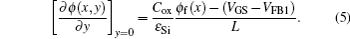
where ϕ (x, y) is the channel potential and ε Si is permittivity of silicon.
The potential profile in the vertical direction in the channel can be approximated by the following parabolic function as follows:[32]

Here, the coefficients C1(x) and C2(x) are the functions of x only, and ϕ f (x) = ϕ (x, 0) is the surface potential at SiO2/Si interface. These coefficients are to be determined by using the following boundary conditions: the surface potential at the source end is

whereas at the drain end is

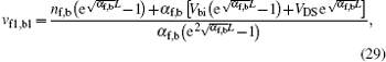
The continuity of the electric flux at the SiO2/Si interface is formulated as
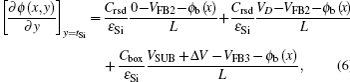
The electric flux at the Si/BOX interface is also continuous, as shown below.
where Vbi is the built-in voltage at the source/drain and Si given by

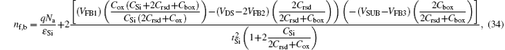
Nd is the doping concentration, ni is the intrinsic carrier concentration in the silicon, VFB1, VFB2, and VFB3 represent the flat-band voltages respectively, [4]VD and VGS are the drain- and gate-to-source bias-voltages, respectively; and, Δ V is the substrate-induced surface potential (SISP) at substrate/BOX interface. The parameter Δ V has been already derived in our previous work.[4] The potential at channel-BOX interface is

which is named a back surface potential. The symbol VSUB refers to the substrate bias voltage.
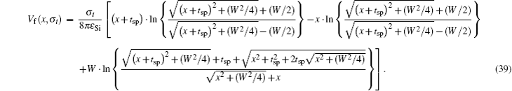
In Eq. (5), Cox is the front channel oxide capacitance per unit length and it is given by[3]

with CSi being the silicon channel capacitance per unit length and it is given by

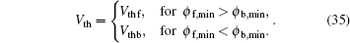
Cbox being the BOX capacitance per unit length and it is given by

Crsd being the recessed source/drain buried-oxide capacitance per unit length and it is given by[4]
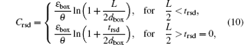
with dbox being the length of source/drain overlap over BOX,

being the effective angle between the two slanted electrodes i.e., back-channel and source/drain extension.[4] It is worth noting here that θ is not always necessarily equal to the physical angle between Re-S/D and back-channel. It can be noticed that θ is π /2 for the Re-S/D SOI MOSFET as dbox = 0, whereas becomes π for the conventional SOI MOSFETs because of trsd = 0. Therefore, with the introduction of parameter dbox, the present model becomes more flexible.
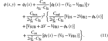
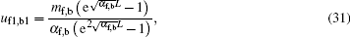
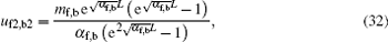
Upon solving the Poisson’ s equation by using Eq. (1) with the help of boundary conditions given by Eqs. (5) and (6) at both front and back surface of silicon body, we obtain the following expression of 2D channel potential ϕ (x, y):
Further, the following two differential equations for ϕ f, b are obtained by using ϕ (x, y) of Eq. (11) in Eq. (1) at y = 0 and y = tSi respectively,

where,
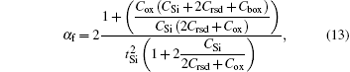
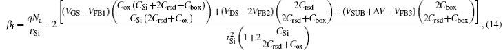
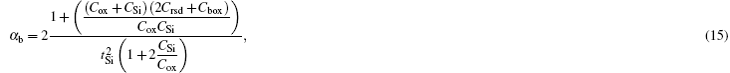
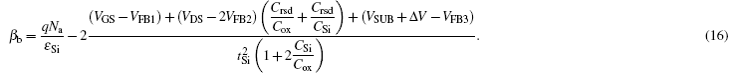
Using the boundary conditions of Eqs. (3) and (4) in solving Eq. (12) gives the following equations for the front and back surface potential

where


The positions (xmin)f, b of the front and back channel minimum surface potentials (virtual cathode potential, ϕ f, bmin) can be obtained by solving

and are determined as
The minimum values of front and back surface potential ϕ f, bmin can be obtained by substituting (xmin)f, b of Eq. (20) into Eq. (11) as

Furthermore, in order to obtain the surface potential including the effect of the fringe capacitance Cbot, the potentials Vf, b(x, σ 1) | source and Vf, b (Lg − x, σ 2) | drain due to the charges on the source and drain regions, respectively, are added to surface potential ϕ f, b and the expression for surface potential Eq. (11) is modified as

The origin and derivation of potential V (x, σ 1, 2) are discussed in Subsection 3.2.
Now, the minimum values of front and back surface potential could be obtained by using Eq. (22). However, the direct derivative of Eq. (22) may lead to a very complicated equation of (xmin)f, b and which in turn gives an implicit equation for threshold voltage. Therefore, assuming that first two terms vary more rapidly than the last two, and the last two terms only modify the minimum values of ϕ minf, b, the following equations for the modified minimum front and back surface potentials could be obtained:
The threshold voltages associated with front and back surfaces of the channel could be obtained by using

where ϕ f is the Fermi potential.
Now, after inserting Eq. (23) into Eq. (24), we obtain the following equations for front and back channel-surface threshold voltages Vthf, b:
where


and finally, the threshold voltage Vth of Re-S/D SOI MOSFETs could be given as follows:[4]
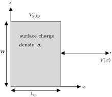
The electric field lines that originate from the bottom of the gate and enter into the source and drain through the spacer induce electrostatic charges in source and drain region. The surface charge density, σ i (i = 1 and 2 for source and drain, respectively) due to fringing electric field lines is given in Fig. 2.[20]
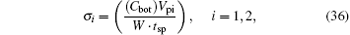
where Vp1 = Vbi − VGS + VFB2 and Vp2 = Vbi + VDS − VGS + VFB2 are the source and drain region potential respectively, W is width of gate and tsp is spacer thickness between gate sidewall and source/drain contacts.
 | Fig. 2. Potential due to uniformly surface-charged plate. |
The parasitic internal fringe capacitances associated with bottom edge of gate electrode can be calculated as[20]

where
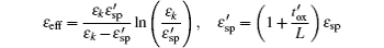
is the effective permittivity of spacer material, ε ox and ε sp are the permittivity values of gate dielectric and spacer material respectively, tox is the gate oxide thickness, and L is the gate length.
Now, the potential at a distance ‘ x’ from uniformly charged plate is given by[20]
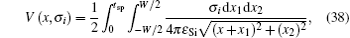
Similarly, the closed form expression of Vb(x, σ i) can be obtained by replacing x1 limits to 
The model accuracy has been improved for ultrathin body structure by adding the following quantum effects induced correction term Δ Vth in the threshold voltage model of Eq. (35).[33, 34]

where Δ E0 is the difference between the first discrete energy level and the lowest conduction band energy level.[33, 34]
In this section, the results obtained from theoretical models of surface potential and threshold voltage are compared with the numerical simulation results. Following the constant current method of threshold voltage extraction, Vth is obtained from the drain current– gate voltage curve by considering the value of the gate voltage at drain current magnitude given by Id = (w/L) × 10− 7 A/μ m, [35] where w and L are width and length of the channel, respectively. It should be noted that the gate oxide thickness shown in the figure is actually the electrical (or effective) thickness 

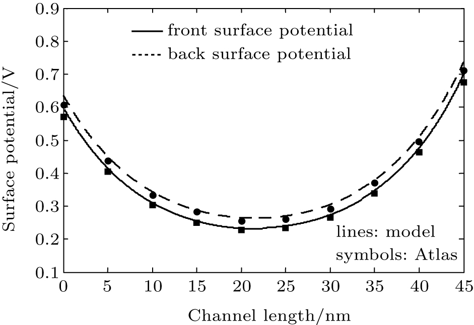 | Fig. 3. Surface potentials versus the channel length in front and back channel. The other device parameters are: ϕ M = 4.8 eV, Na = 1016 cm− 3, Nd = 1020 cm− 3, tbox = 200 nm, tSi = 8 nm, trsd = 30 nm,  |
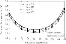
Figure 4 displays the back surface potential variation against the channel length for different values of gate dielectric constant (ε k). The minimum of the back surface potential is found to increase as the gate dielectric constant increases. This increase in the minimum of back surface potential leads to the lowering of the source-channel barrier height, which subsequently results in change in the threshold voltage. It could be safely concluded here that fringing field lines considerably modulate the threshold voltage of a Re-S/D SOI MOSFET.
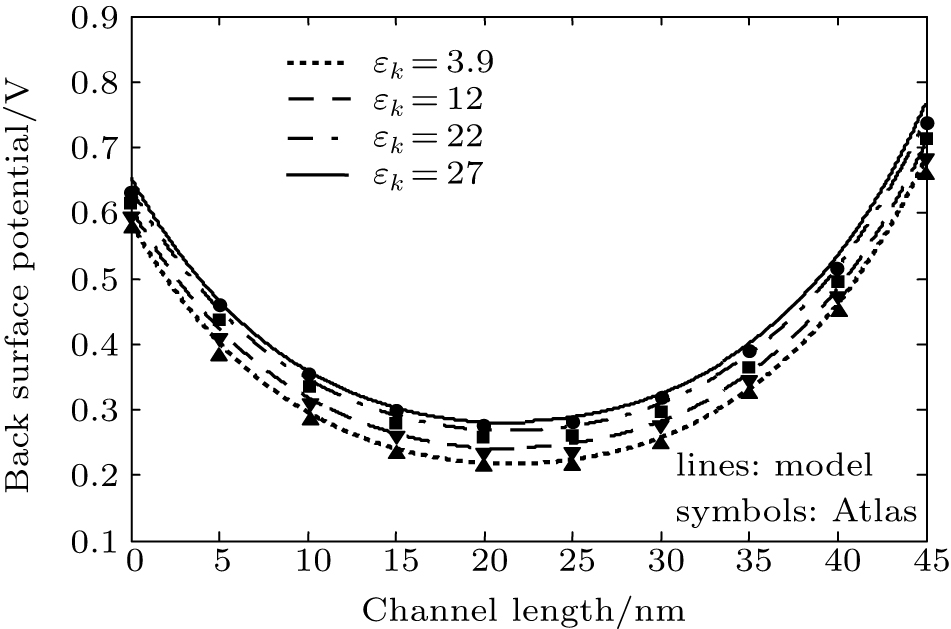 | Fig. 4. Back surface potentials versus channel length for various values of gate-dielectric constant (ε k). The other device parameters are the same as those in Fig. 3. |
Figure 5 shows the threshold voltages of Re-S/D SOI MOSFETs versus channel length for the BOX thickness values of 100 nm and 200 nm. It is observed that the device with a thinner BOX has a higher threshold voltage and is also less prone to short-channel effects (SCEs).
 | Fig. 5. Threshold voltages versus gate length for buried oxide thickness values. The other device parameters are the same as those in Fig. 3. |
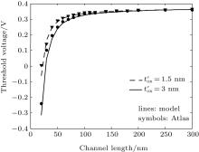
Figure 6 shows the variations of threshold voltage with channel length for the values of oxide thickness, 
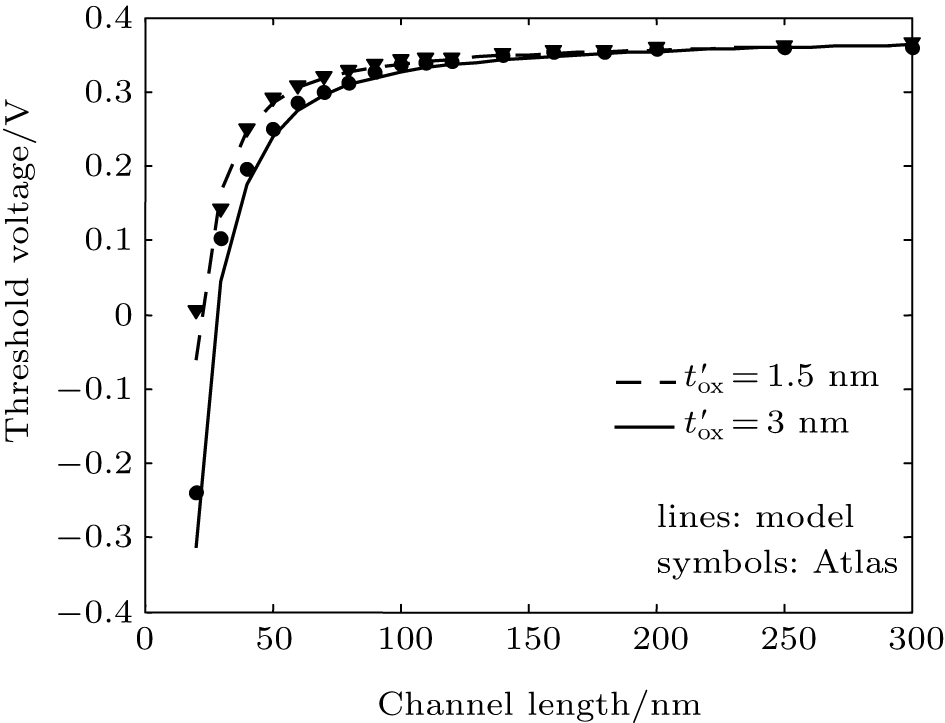 | Fig. 6. Threshold voltages versus gate length for different gate oxide thickness values. The other device parameters are the same as those in Fig. 3. |
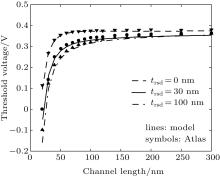
Figure 7 shows the variations of threshold voltage with channel length while trsd serves as a variable parameter with HfO2 as a dielectric material. The selected thickness values for source and drain penetration in the BOX are trsd = 0 nm, 30 nm, and 100 nm. It should be noted that for trsd = 0 the device acts as a conventional SOI MOSFET, and as a result, the threshold voltage remains higher than the case of trsd = 30 nm and 100 nm. This may be attributed to the fact that at lower channel doping, the back surface may turn inverted at first if the channel length is too short (L < 70 nm). And, since the back channel is partially controlled by source and drain extension, the subthreshold characteristics of the device are deteriorated.
 | Fig. 7. Threshold voltages versus gate length for different recessed oxide thickness values. The other device parameters are the same as those in Fig. 3. |
Figure 8 shows the variation of threshold voltage with the dielectric constant of gate-dielectric, whereas the other device parameters are ϕ M = 4.6 eV, Na = 1016 cm− 3, Nd = 1020 cm− 3, tSi = 8 nm, trsd = 30 nm, Nd = 200 nm, VGS = 0.1 V, and L = 45 nm. The threshold voltage of the device is found to decrease with the increase of dielectric constant. This observation is in line with the case of Fig. 4, where a minimum of surface potential is found to increase with the increase of the dielectric constant, ε k. It should be noted that the source channel barrier height becomes lower with the increase of the minimum of the surface potential and, as a result, charge carriers from the source may be easily injected into the channel region, which is an indication of lowering the threshold voltage.
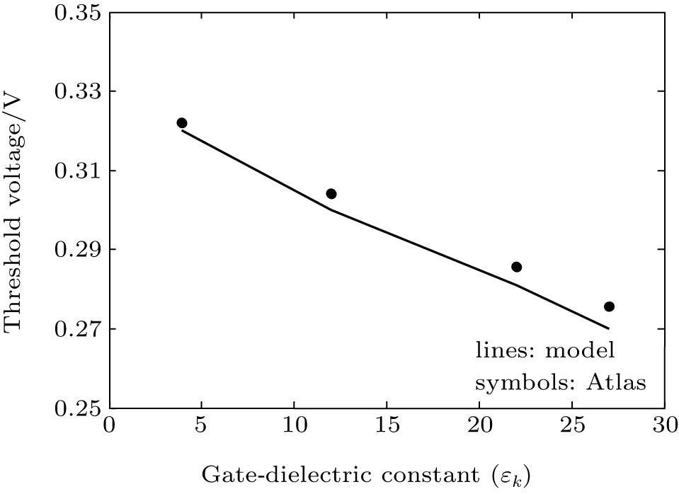 | Fig. 8. Threshold voltage versus gate-dielectric constant (ε k). The other device parameters are described in the text. |
A 2D threshold voltage model of FD recessed-source/drain (Re-S/D) SOI MOSFET with high-k gate dielectric material is presented for the first time. The present model includes the effect of high-k dielectric induced fringing field lines in terms of capacitance Cbot, which appears to be due to the electrostatic interaction between the bottom of the gate-electrode and source/drain. It is found that the present model predicts the threshold voltage of Re-S/D SOI MOSFET correctly in wide ranges of gate-dielectric materials and other device parameters. The derived model results are compared with simulation results which are obtained from ATLASTM (Silvaco), showing that they are in good agreement with each other in a wide variation range of device parameters.
| 1 |
|
| 2 |
|
| 3 |
|
| 4 |
|
| 5 |
|
| 6 |
|
| 7 |
|
| 8 |
|
| 9 |
|
| 10 |
|
| 11 |
|
| 12 |
|
| 13 |
|
| 14 |
|
| 15 |
|
| 16 |
|
| 17 |
|
| 18 |
|
| 19 |
|
| 20 |
|
| 21 |
|
| 22 |
|
| 23 |
|
| 24 |
|
| 25 |
|
| 26 |
|
| 27 |
|
| 28 |
|
| 29 |
|
| 30 |
|
| 31 |
|
| 32 |
|
| 33 |
|
| 34 |
|
| 35 |
|