

Electrical properties of zinc-oxide-based thin-film transistors using strontium-oxide-doped semiconductors
[Wu Shao-Hanga), b) , Zhang Nana) , Hu Yong-Shenga) , Chen Hongc) , Jiang Da-Penga) , Liu Xing-Yuan†a)  ]
]
]
|
|


†Corresponding author. E-mail: liuxy@ciomp.ac.cn
*Project supported by the National Natural Science Foundation of China (Grant No. 6140031454) and the Innovation Program of Chinese Academy of Sciences and State Key Laboratory of Luminescence and Applications.
Strontium-zinc-oxide (SrZnO) films forming the semiconductor layers of thin-film transistors (TFTs) are deposited by using ion-assisted electron beam evaporation. Using strontium-oxide-doped semiconductors, the off-state current can be dramatically reduced by three orders of magnitude. This dramatic improvement is attributed to the incorporation of strontium, which suppresses carrier generation, thereby improving the TFT. Additionally, the presence of strontium inhibits the formation of zinc oxide (ZnO) with the hexagonal wurtzite phase and permits the formation of an unusual phase of ZnO, thus significantly changing the surface morphology of ZnO and effectively reducing the trap density of the channel.
Thin-film transistors (TFTs) based on zinc oxide (ZnO) semiconductors, especially zinc indium oxide (ZnInO), are of great interest for transparent electronic applications due to their favorable characteristics, including high electron mobility, high transparency in the visible light region, excellent electrical stability, and superior uniformity over a large area.[1– 5] However, the use of indium presents limitations to these characteristics due to the use of this rare element in transparent electrodes, which are currently in high demand.[6– 8] Recently, great efforts have been made to develop ZnO-based TFTs without adding any rare elements. However, as-deposited ZnO films tend to have a high carrier concentration, which results in poor carrier control through the applied gate voltage and, consequently, a low on/off ratio.[4, 9, 10]
In an effort to achieve better carrier control in ZnO-based TFT, there have been many attempts to suppress carrier concentration without reducing mobility, including adding carrier suppressors, such as gallium (Ga), hafnium (Hf), zirconium (Zr), and anthanum (La).[5, 11– 13] Carrier suppression is achieved in these materials because the oxygen vacancies and carrier generation are prevented, to some extent, from forming due to the formation of stronger chemical bonds with oxygen than Zn and In ions and an increase in the donor binding energy.[5, 12, 14] In general, stronger chemical bonds with oxygen lead to a wider band gap for the corresponding oxides, which has been proposed as a primary factor for consideration. Electronegativity may also play a role in this kind of material, especially in amorphous ZnO films.[13, 15]
As shown in Table 1, suppressors, such as Ga2O3, HfO2, ZrO2, and La2O3, have wider band gaps than ZnO and In2O3, in line with typical bond dissociation energies in diatomic molecules. However, the Pauling electronegativities of both In and Zn are smaller than that of Ga, but larger than those of Hf, Zr, strontium (Sr), or La. This indicates that the band gap is more related to selecting a suppressor. Further, considering the valence state, only the Sr ion has a valence state equal to that of Zn ion, making Sr unfavorable as a donor for ZnO.
| Table 1. Comparisons of band gap and Pauling electronegativity among different elements. |
In this study, we incorporate Sr into the ZnO semiconductor to suppress the carrier concentration and thereby improve the TFT on/off ratio. The results show that a strontium-zinc-oxide (SrZnO) TFT has a higher on/off ratio than a ZnO TFT under the same conditions. In addition, the off-state current of the ZnO TFT is dramatically reduced by three orders of magnitude after adding Sr. SrZnO TFT device displays an optimal performance with an on/off ratio of 105, a mobility of 0.05 cm2/V· s, and a threshold voltage of 24.6 V.
Sputtering is a commonly used technique for deposition of oxide-based TFTs.[20] However, the significant processing required for high-quality sputtering targets is burdensome.[21] Transparent conductor oxide films can be deposited by an ion-assisted electron beam evaporation technique, which is simpler than sputtering but seldom reported for the films used in TFT active layers.[22– 25] Therefore, we prepare SrZnO channel layers for TFTs by using the ion-assisted electron beam evaporation. A schematic of the TFT is shown in Fig. 1.
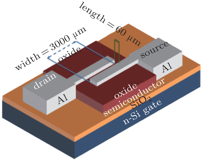 | Fig. 1. Schematic diagram of the TFT (channel width = 3000 μ m and channel length = 60 μ m). |
The SrZnO target for electron beam evaporation was fabricated by mixing ZnO (99.99%) and SrO (99.99%) powders at a molar ratio of Zn:Sr = 1:1. The powders were ground for 2 h to ensure intensive mixing. SrZnO blocks with a 2.5-cm diameter and 3-cm height were fabricated by using a compression molding press operating at a pressure of 8 MPa. Subsequently, the shaped SrZnO blocks were sintered in a muffle furnace at 1250 ° C for 4 h. A pure ZnO target was also fabricated by using the same technique. The purpose of high-temperature processing is to release the oxygen molecules from the mixture. If oxygen molecules were released during deposition instead, the working pressure would increase and the evaporation process would be poorly controlled.
Clean substrates composed of a heavily doped n-type silicon with 300-nm thermally oxidized SiO2 were positioned 60 cm above the SrZnO or ZnO target in the chamber, and then the background pressure was reduced to a value lower than 2.0× 10− 3 Pa. During film deposition, the chamber was flushed with O2 gas to maintain a working pressure of 4.0× 10− 2 Pa. An end-Hall ion source operating at an anode voltage of 150 V, an anode current of 2 A, and a cathode current in a range of 12 A– 15 A was used to facilitate the deposition. The rate of deposition, which was monitored in situ by using a thin-film deposition controller, was controlled to about 0.2 nm/s until the film thickness reached 50 nm. Then, the samples were annealed for 20 min at 250 ° C in air. Immediately after this, aluminum (Al) was evaporated as the source/drain electrodes by using masking patterns to form the channel region with a length of 60 μ m and a width of 3000 μ m. Finally, the samples were annealed in air at 250 ° C for 60 min to produce the switching characteristics.
The electrical characteristics of these samples were measured by using a semiconductor parameter analyzer (Keithley 4200). X-ray diffraction (XRD) patterns were obtained by using a powder diffractometer (D8 Focus, Bruker, Germany). Atomic force microscopy (AFM) was performed with an AFM (SPA-9700, Shimadzu) in phase mode. Energy dispersive x-ray (EDX) analysis was performed using a GENE SIS2000 XMS 60S (EDAX Inc.). All of the measurements were performed at room temperature in ambient air.
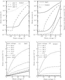
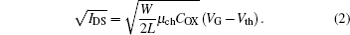
The transfer characteristics of a typical n-type TFT, obtained by measuring the source-to-drain current (IDS) with respect to the gate voltage (VG), are shown in Figs. 2(a)– 2(b). Annealings are carried out under different temperatures, and the data suggest that annealing at 250 ° C results in the best transfer characteristics. As figure 2(b) indicates, the drain current of the ZnO TFT is always larger than that of the SrZnO TFT when the gate voltage is between − 40 V and 60 V. However, the on/off ratio of the SrZnO TFT is larger than that of the ZnO TFT, owing to the difference in off-state current between the two materials. These results indicate that the ZnO active layer is more conductive than the SrZnO one, but the SrZnO active layer allows better control of conductivity. The IDS and VG for representative TFTs in the saturation regime under the condition VG ≥ Vth and VDS > VDSAT are related through the following equation:

where μ ch is the mobility in the channel, COX is the capacitance per unit area of the gate dielectric, W is the width of the channel, L is the length of the channel, VDSAT is the saturation voltage, and VDS is the voltage between the drain and source. Equation (1) can be used to calculate the channel mobility and rearranged as follows:
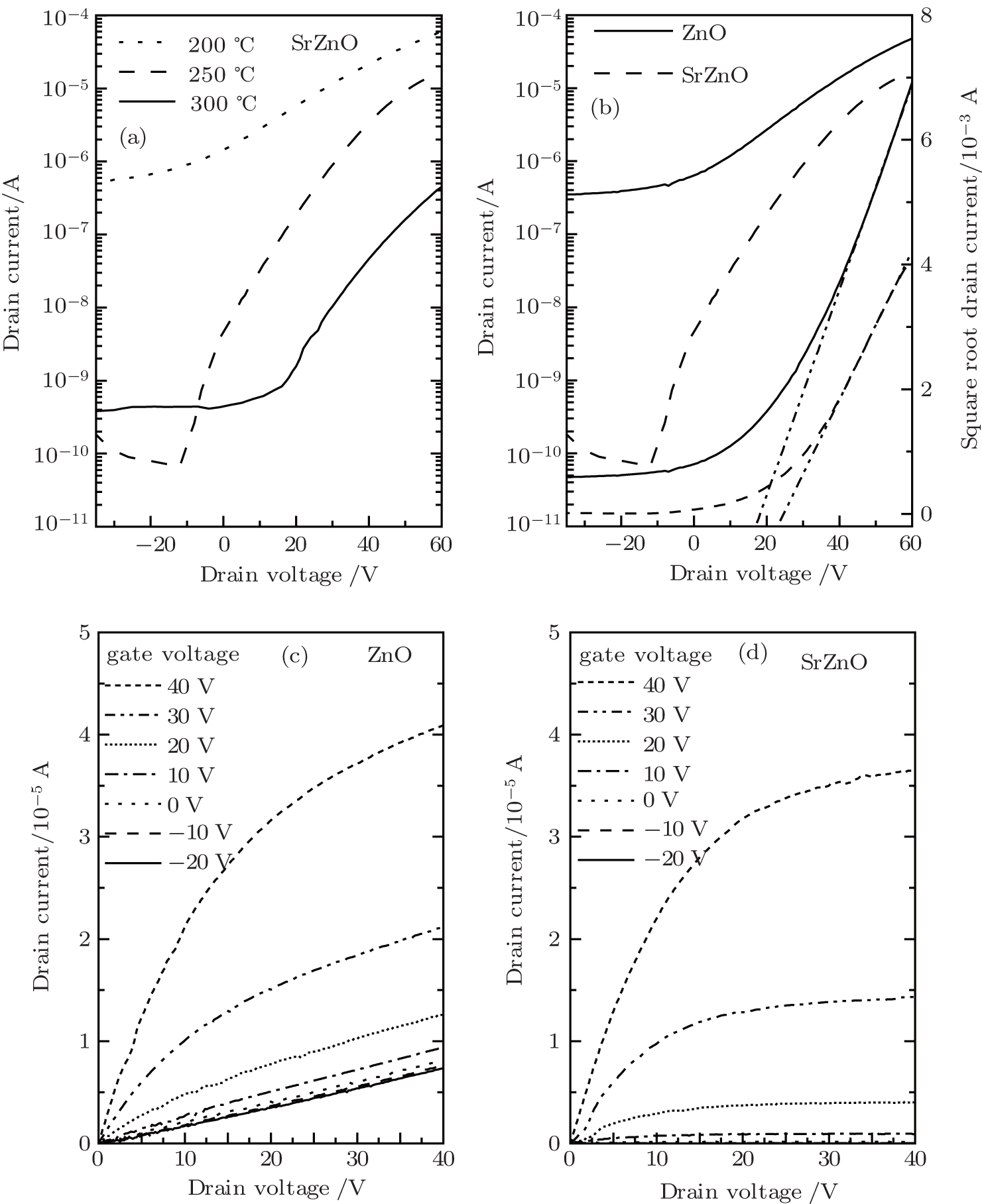 | Fig. 2. (a) Transfer characteristics for the SrZnO TFT for being annealed at different temperatures (VDS = 5 V). (b) Transfer characteristics for the ZnO TFT and the SrZnO TFT (after being annealed at 250 ° C, VDS = 5 V). (c) Output curves of the ZnO TFT (after annealing at 250 ° C). (d) Output curves of SrZnO TFT (after being annealed at 250 ° C). |
Figure 2 shows the curves of the square root drain current versus VG. The mobility is calculated by finding the slope in the gate voltage range from 40 V to 60 V; the calculated values are 0.095 cm2/(V· s) and 0.050 cm2/(V· s) for ZnO and SrZnO, respectively. Furthermore, the threshold voltages can be obtained by a linear extrapolation in the same gate voltage region, which are found to be 18.2 V and 24.6 V for ZnO and SrZnO, respectively. Therefore, the SrZnO TFT requires a larger gate voltage to generate carriers than the ZnO TFT.
In addition, we can estimate the trap density from the subthreshold slope using the following equation:
where q is the electron charge, kB is the Boltzmann constant, T is the absolute temperature, I is the source to drain current, COX is the capacitance per unit area of the gate dielectric, and N is the total density of traps of the channel layer and interface with SiO2. Here, the subthreshold slopes are determined from the transfer characteristics between 50 V and 60 V using S = (d log10IDS/dVGS)− 1, and found to be 40.4 V· dec− 1 and 36.0 V· dec− 1 for the ZnO TFT and the SrZnO TFT, respectively. Using these slopes, the corresponding trap densities are calculated to be 4.99× 1013 cm− 2· eV− 1 and 4.44× 1013 cm− 2· eV− 1, respectively. This is direct evidence that the presence of Sr is an effective way to reduce the ZnO-based channel related trappings in these devices. The relevant data are summarized in Table 2.
| Table 2. Comparison of electrical characteristic between ZnO and SrZnO TFT. |
The output characteristics curves are shown in Figs. 2(c) and 2(d). The IDS increases with the increase of gate bias voltage (VGS), signifying that the free electrons are generated by a positive VGS and that the devices are n-type transistors. According to Ohm’ s law, the channel’ s resistance can be calculated as Rch = U/I, where Rch, U, and I are the resistance of channel, source-to-drain voltage and source-to-drain current, respectively. As in the results for VGS and VDS, the ZnO TFT exhibits a larger saturation current than the SrZnO TFT. Therefore, the Rch of ZnO is smaller than that of SrZnO, particularly for negative value of VGS. When VGS is between − 10 V and − 20 V, the resistance of the SrZnO channel is large enough to pinch-off the channel and the IDS is essentially constant. However, the IDS of ZnO TFT increases with VDS increasing, signifying a poor off-state. Therefore, these results are consistent with those described above and they show that Sr is an effective carrier suppressor in a ZnO-based semiconductor.
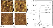
To explore the physical differences between ZnO and SrZnO, we measure the channel morphologies by using AFM, these results are shown in Figs. 3(a)– 3(d). Numerous particles with diameters of about 100 nm– 120 nm can be observed in the ZnO films. Annealing significantly increases the number of particles as can be seen in Figs. 3(a) and 3(b). Consequently, the roughness of the surface increases from 3.1 nm to 4.2 nm. The distribution of surface relief is shown to the right of each AFM image and indicates that larger fluctuations are present in the annealed ZnO films. This is likely to be due to the growth of grains under thermal treatment at 250 ° C. We prepare 300-nm SrZnO films under the same conditions in order to obtain the XRD spectra, which are shown in Fig. 3(e). We see the primary peak at about 34° , which is identified with the (002) peak of the hexagonal-wurtzite-phase ZnO crystal structure (JCPDS card No. 36-1451). Specifically, the (002) peak intensity slightly retrogresses and its position is shifted from 34.12° to 34.16° after being annealed, a shift towards the reference value of 34.421° in JCPDS card No. 36-1451. We determine, therefore, that the particles with sizes of about 100 nm– 120 nm have the preferable hexagonal wurtzite crystal structure and that the annealing process is conducive to the growth of these particles and the shift of (002) peak position.
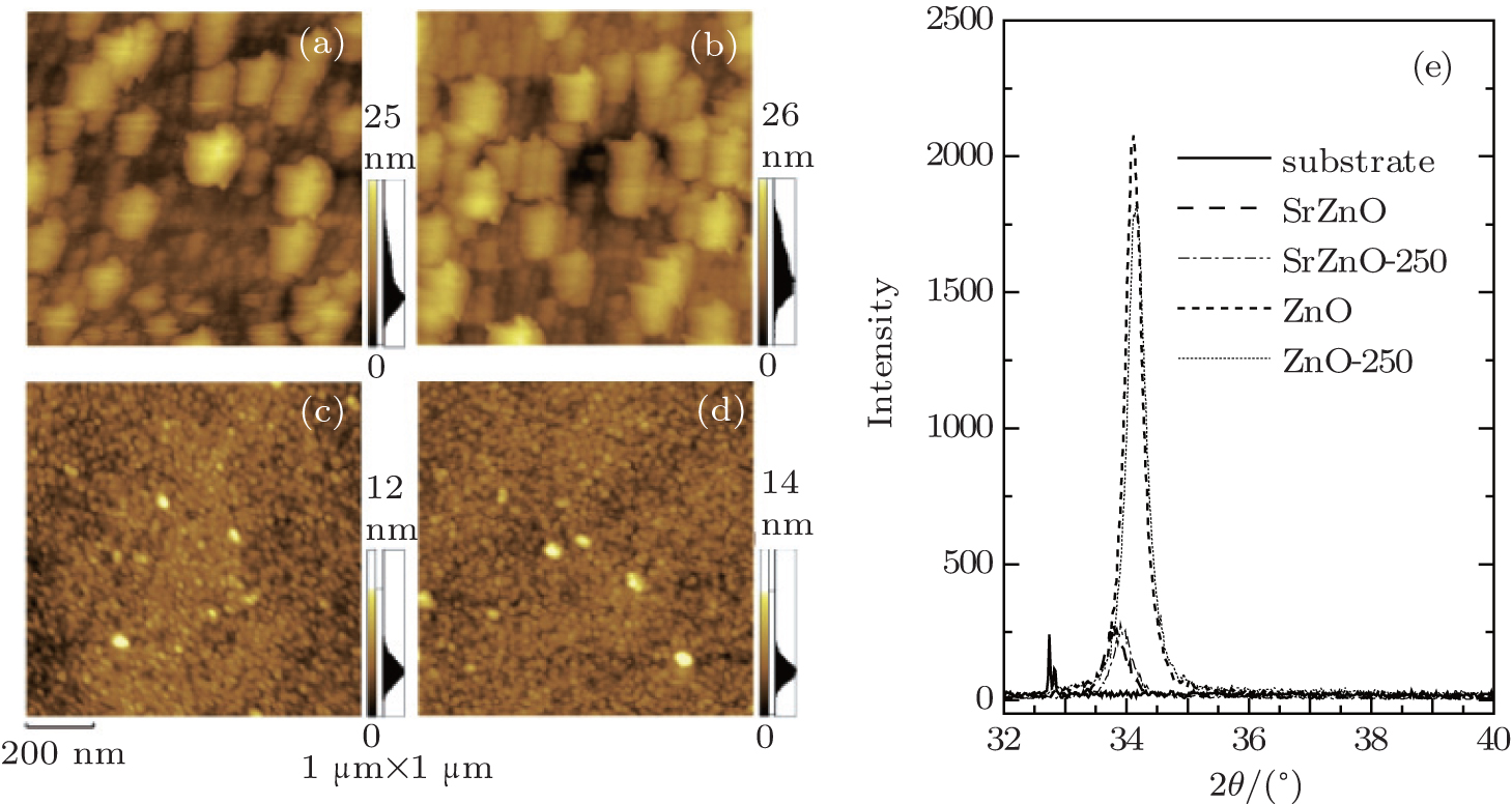 | Fig. 3. (a) AFM image of untreated ZnO film. (b) AFM image of ZnO film annealed at 250 ° C. (c) AFM image of untreated SrZnO film. (d) AFM image of SrZnO film annealed at 250 ° C. (e) XRD patterns for the different samples. |
As shown in Figs. 3(c) and 3(d), the channel morphologies of the SrZnO films are significantly different from those of ZnO films. The particle sizes in SrZnO are only about 21.5 nm and 23.9 nm before and after being annealed at 250 ° C, respectively, and the roughness values of surfaces are 1.3 nm and 1.4 nm, respectively. Therefore, the presence of Sr has significant implications for the film morphology.
Unexpectedly, the XRD spectrum in Fig. 3(e) shows that the primary peaks for SrZnO films are located at 33.78° and 33.90° before and after being annealed, respectively. These peaks only agree with an unusual phase of ZnO (JCPDS card No. 21-1486), which typically appears in samples prepared by chemical reaction and has a reference value of 33.665° [26– 29]
As shown in Fig. 4(a), the XRD pattern of SrZnO target has a series of diffraction peaks, most of which agree with the characteristic peaks of SrZnO (JCPDS card No. 41-0551). In addition, there are three peaks consistent with those of ZnO (JCPDS card No. 36-1451) and specially marked by the word ‘ ZnO’ . The significant difference between SrZnO target and pure ZnO target is observed via SEM in Figs. 4(b) and 4(c). The ZnO target has a layered structure, but the SrZnO target is composed of messy small pieces. This indicates that the incorporated Sr is capable of changing the target structure. The Sr content and Zn content in the SrZnO film and target are checked via energy dispersive x-ray analyses as shown in Figs. 4(d) and 4(e). The molar ratios of Sr:Zn are 0.95:1 and 1.03:1 for SrZnO film and target, respectively. This composition segregation results mainly from a small amount of decomposition of raw material in the evaporation process.
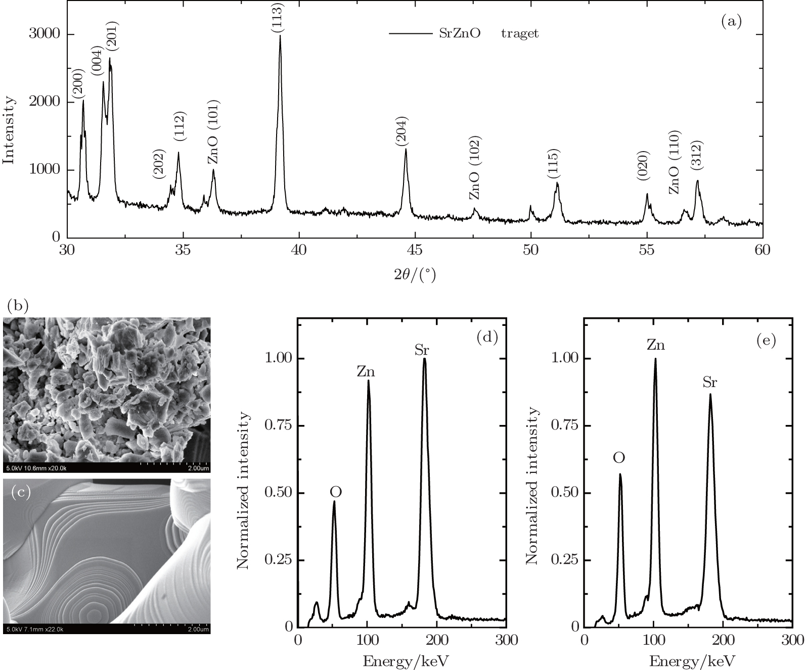 | Fig. 4. (a) XRD pattern of SrZnO target. (b) SEM image of SrZnO target. (c) SEM image of ZnO target. (d) Energy dispersive x-ray spectrum of SrZnO target. (e) Energy dispersive x-ray spectrum of SrZnO film. |
The SrZnO semiconductors are prepared for TFT devices through ion-assisted electron beam evaporation. The greatly reduced off-state current in SrZnO TFT as compared with that in ZnO TFT suggests that Sr is an effective carrier suppressor in a ZnO semiconductor. Furthermore, the results show that Sr is capable of changing the surface morphology of ZnO film, resulting in the presence of an unusual phase of ZnO and the suppression of the growth of the common polycrystalline structure of ZnO. The carrier suppressor plays a considerable role in improving the uniformity and stability of the device, which is important for large scale fabrication.[30] Although the mobility of device drops off clearly, it can be improved to an application level via optimizing the device structure or doping another element, such as Tin, which will be reported in our following work.[9, 11, 31]
| 1 |
|
| 2 |
|
| 3 |
|
| 4 |
|
| 5 |
|
| 6 |
|
| 7 |
|
| 8 |
|
| 9 |
|
| 10 |
|
| 11 |
|
| 12 |
|
| 13 |
|
| 14 |
|
| 15 |
|
| 16 |
|
| 17 |
|
| 18 |
|
| 19 |
|
| 20 |
|
| 21 |
|
| 22 |
|
| 23 |
|
| 24 |
|
| 25 |
|
| 26 |
|
| 27 |
|
| 28 |
|
| 29 |
|
| 30 |
|
| 31 |
|