

A novel diode string triggered gated-PiN junction device for electrostatic discharge protection in 65-nm CMOS technology
[Zhang Li-Zhong, Wang Yuan† , Lu Guang-Yi, Cao Jian, Zhang Xing]
, Lu Guang-Yi, Cao Jian, Zhang Xing]
|
|


†Corresponding author. E-mail: wangyuan@pku.edu.cn
*Project supported by the National Basic Research Program of China (Grant No. 2011CBA00606).
A novel diode string-triggered gated-PiN junction device, which is fabricated in a standard 65-nm complementary metal-oxide semiconductor (CMOS) technology, is proposed in this paper. An embedded gated-PiN junction structure is employed to reduce the diode string leakage current to 13 nA/μm in a temperature range from 25 °C to 85 °C. To provide the effective electrostatic discharge (ESD) protection in multi-voltage power supply, the triggering voltage of the novel device can be adjusted through redistributing parasitic resistance instead of changing the stacked diode number.
Electrostatic discharge (ESD) continues a serious reliability issue in the semiconductor industry. This concern is intensified with the critical dimension entering into a nanometer scale, which introduces more challenges to ESD protection design.[1, 2] For GHz radio frequency (RF) integrated circuit (IC) applications, the ESD protection device should meet the requirement of balancing between low parasitic capacitance and high ESD robustness. Diode strings are widely used to clamp the ESD overstress voltage between power lines because the diode in the forward-biased condition is able to sustain a higher ESD level than that in the reverse-biased condition.[3– 5] In addition, diode strings can result in a total parasitic capacitance smaller than that of a single diode, which provides a reasonable solution for RF ESD protection design. However, diode strings are commonly built in floating n-wells in p-type substrate complementary metal-oxide semiconductor (CMOS) process and are actually PNP transistors because the common grounded p-type substrate acts as a collector.[4] The leakage current of diode strings is large at room temperature due to the Darlington effect, which is exponentially worse as temperature rises. In order to restrain Darlington effect in diode strings, some modified circuits with auxiliary triggering designs[4, 6] are introduced, such as boosted, cladded, and snubber-clamped diode strings, which increase circuit complexity and layout cost. An extra triple-well process is adopted to avoid the vertical PNP bipolar effect[7] with the cost of some extra process masks. In this paper, a novel diode string device, fabricated in a standard 65-nm CMOS technology without using additional masks or processing steps, is proposed with an embedded gated PiN junction device to solve the leakage current issue. The novel structure, which is named a diode string-triggered gated-PiN junction (DST-gPiN) device, has an alterable triggering voltage to meet different ESD protection requirements by redistributing the parasitic resistance throughout the whole device structure. The parasitic resistance redistribution can be realized through critical parameter adjustments, which will not bring in extra leakage current compared with the traditional method of altering the stacked diode number. The conflict between low leakage current during normal operation (“ increasing the stacked diode number” ) and proper ESD triggering voltage (“ decreasing the stacked diode number” ) has been well managed. Finally, the turn-on time variation of the proposed device is also discussed.
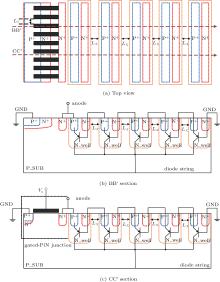
Figure 1(a) illustrates the top view of the proposed DST-gPiN device. The BB′ and CC′ cross-sectional views of the device are shown in Figs. 1(b) and 1(c), respectively. Usually, when the current spreads in the P+ /N-well diode string, the current amplification effect of the vertical parasitic p– n– p bipolar transistor will cause a very serious substrate leakage current. In the novel DST-gPiN device, a gated-PiN junction (formed by P+ /P_SUB/N+ junction) is added on the left of the diode string to suppress the leakage current flowing from the anode to the cathode. The embedded gated-PiN junction has 12% layout area cost compared with the pure diode strings. A tied structure is utilized between the N+ region in the gated-PiN junction and the first P+ region of the diode string. The potential of the floating N-well region, adjacent to the N+ region in the gated-PiN junction, will be increased due to the mentioned tied structure. The voltage drop will decrease from the emitter (P+ region) to the base (floating N-well region) of the parasitic p– n– p bipolar transistor in the first diode. Owing to the lowered emitter injection efficiency, the substrate leakage current will be effectively reduced before the whole device structure turns on in an ESD event. Moreover, the triggering voltage of the novel DST-gPiN device can be altered by adjusting the parasitic resistance throughout the whole device, which is realized by two methods. One method is to redistribute the series resistance between two base regions of adjacent parasitic p– n– p bipolar transistors, which is a linear function of the distance between N-wells, LX. The other method is to change the distance between gate polysilicon strips, LY, with the total device gate width fixed. The larger distance results in a lower strip number, which will finally be incorporated into a larger contact resistance. The resistance distribution throughout the whole DST-gPiN device will determine the current flow assignments, which makes the triggering voltage adjusted in order to meet different ESD protection requirements.
 | Fig. 1. Novel DST-gPiN device structure realized in P-substrate CMOS technology, showing (a) top view, (b) BB′ section view, and (c) CC′ section view. |
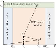
The operation of each ESD protection device is illustrated by the current– voltage (I– V) curve described in Fig. 2. The ESD design window is between the normal operating region and the gate breakdown region. For an effective ESD protection design, it is required that the triggering voltage Vt1 at point A should satisfy the following rule:

where BVGate represents the gate breakdown voltage of the core circuit and VDD is the power supply voltage. In order to avoid latch-up issue existing in CMOS process, the holding voltage Vh at point B should exceed VDD. But it is not desirable to increase Vh, owing to the induced high ESD heat. Thus, the Vh is required to satisfy the following condition:

The point C is also an important parameter for ESD design in the second breakdown region, and the second breakdown current It2 denotes the ESD protection level. With the development of the CMOS technology, the ESD design window is smaller. This makes it more difficult to design an effective protection scheme. In this 65-nm CMOS technology, the BVGate is about 6 V and the power supply voltage is 2.5 V.
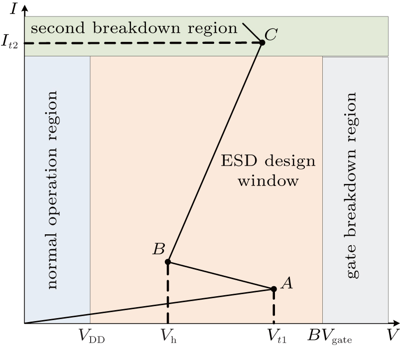 | Fig. 2. ESD design window. |
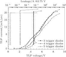
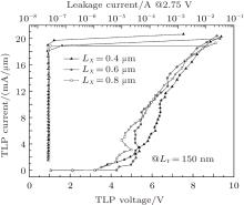
Figure 3 illustrates the triggering voltage engineering technique by showing transmission line pulse (TLP) I– V characteristics of three DST-gPiN devices with different stacked diodes at LX = 0.8 μ m and LY = 150 nm. The TLP generator will produce 100-ns wide rectangular pulses with 10-ns rise time, which corresponds to HBM ESD test.[8] Because of Darlington effect of diode strings, when the current gain β of the parasitic vertical p– n– p transistor is equal to one or even larger, the triggering voltage will not be linearly increased as the stacked diode number increases. In contrast, an unexpected leakage current will exponentially increase when the stacked diode number decreases. The DST-gPiN device with five stacked diodes is selected to obtain the lowest leakage current. Its triggering voltage and holding voltage are both equal to 3.2 V, which meets the requirements for an ESD design window in a 65-nm CMOS technology.
 | Fig. 3. DST-gPiN triggering voltage engineering, showing the measured TLP-IV characteristics of DST-gPiN with various diode numbers. |
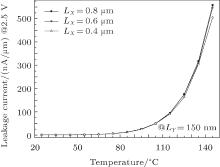
The measured leakage current curves for the DST-gPiN device with various values of LX are compared with those in Fig. 4, where the stacked diode number is five. When the environmental temperature rises from 25 ° C to 85 ° C, the leakage current is successfully reduced below 13 nA/μ m and it will not exceed 550 nA/μ m even at a temperature of 150 ° C under 2.5-V power supply voltage on the anode. From Fig. 4, it can also be found that the LX variation has almost no influence on the leakage current.
 | Fig. 4. Measured leakage currents for the DST-gPiN device versus environmental temperature for different values of Lx. |
In Fig. 5, ESD performances of the DST-gPiN device with various values of LX are investigated under TLP test when the stacked diode number is five and LY is fixed at 150 nm. As illustrated in Fig. 1, the increase of LX linearly increases the series resistance between two base regions of adjacent parasitic p– n– p bipolar transistors. The triggering voltage adjustment is realized through the parasitic resistance redistribution. From Fig. 4, compared with the traditional method of changing stacked diode number, proper triggering voltage adjustment of the DST-gPiN device is achieved by critical parameter LX modification without extra leakage current to satisfy different ESD protection requirements.
 | Fig. 5. DST-gPiN triggering voltage engineering, showing TLP-IV characteristics of DST-gPiN with various values of LX. |
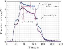
The DST-gPiN devices with the above three values of LX are tested to ascertain the effects of parasitic resistance on the turn-on time of the devices as shown in Fig. 6. Since the linear regression lines used to estimate the asymptote are visible in Fig. 6, there is a huge overlap between the curves of LX = 0.4 μ m and LX = 0.8 μ m. The critical parasitic parameters (such as capacitance and resistance), which result in a lower triggering voltage, will finally be incorporated into a longer turn-on time.
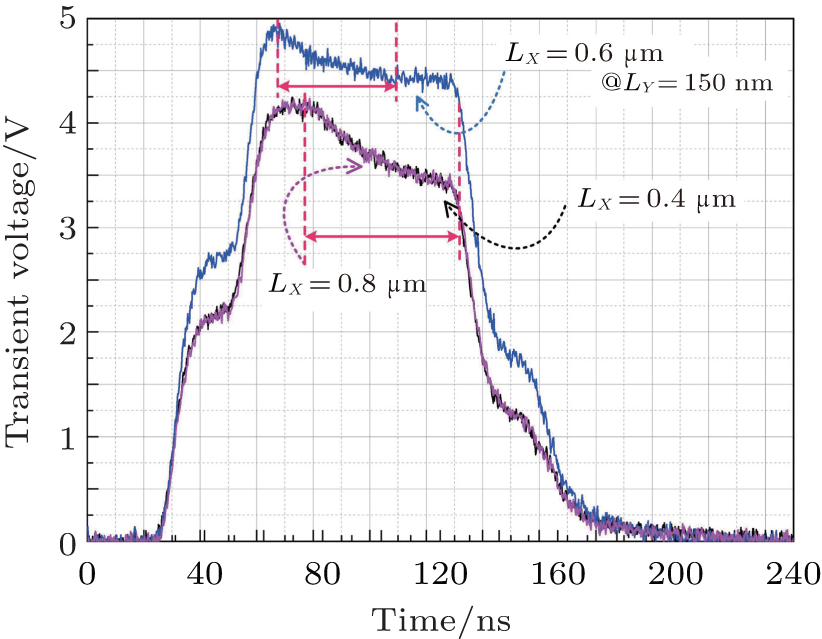 | Fig. 6. Turn-on behaviors of DST-gPiN device structure for various values of LX. |
The DST-gPiN devices with LY values of 150 nm, 200 nm, and 250 nm are tested to investigate the influence of LY on the triggering voltage. The value of LX is fixed at 0.8 μ m. As shown in Fig. 7, the adjustable triggering voltage is obtained through modifying the value of LY. It can also be observed that a larger LY results in a smaller leakage current. Thus, the device structure with LY value of 250 nm is most desirable for its proper triggering voltage and the lowest leakage. In addition to LX, the adjustment of critical parameter LY also provides an alternative solution to redistribute the parasitic resistance without bringing in extra leakage current.
 | Fig. 7. DST-gPiN triggering voltage engineering, showing the TLP-IV characteristics of DST-gPiN with various values of LY. |
In order to ascertain the effect of LY on the turn-on time of the novel DST-gPiN device structure, the same values of LY are selected when LX is fixed at 0.8 μ m in these devices. Figure 8 illustrates the transient waveforms for the DST-gPiN device with three values of LY, the asymptote estimated using the linear regression lines is presented. The novel structure with LY value of 200 nm exhibits the shortest turn-on time and a similar correlation between turn-on time and triggering voltage in Fig. 6 is also obtained, as expected.
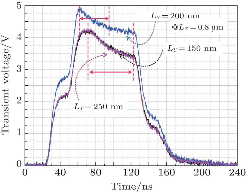 | Fig. 8. Turn-on behaviors of DST-gPiN device structure for various values of LY. |
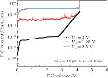
Figure 9 shows a comparison of the I– V curves of the novel DST-gPiN device structure under different voltage levels on the node VG in the ESD-detection circuit. These observations show that increasing the VG is not able to reduce the triggering voltage of the DST-gPiN device, but switches on the gated-PiN junction to conduct the current[9– 11] before the DST-gPiN device reaches its triggering point during ESD stress conditions.
 | Fig. 9. The I– V curves of the novel DST-gPiN device structure under different bias voltages at VG. |
A novel DST-gPiN device, fabricated in a 65-nm CMOS technology, is proposed in this paper. Compared with the traditional P+ /N-well diode strings, the embedded gated-PiN junction on the left side achieves a low leakage current. Instead of adopting the traditional means of altering the stacked diode number, the triggering voltage adjustment of the DST-gPiN device can be realized through critical dimension modification without meeting the requirements of extra leakage current for ESD protection in multi-voltage circuits. Based on the experimental results, the correlation between the turn-on time and triggering voltage is also revealed. When an ESD event occurs, the gate voltage of the novel DST-gPiN device will increase due to the coupled ESD-detection circuit and switch on the PiN junction to conduct ESD current before reaching its triggering point.
| 1 |
|
| 2 |
|
| 3 |
|
| 4 |
|
| 5 |
|
| 6 |
|
| 7 |
|
| 8 |
|
| 9 |
|
| 10 |
|
| 11 |
|