


An improved GGNMOS triggered SCR for high holding voltage ESD protection applications
[Zhang Shuai†a)  , Dong Shu-Rong
b) , Wu Xiao-Jinga) , Zeng Jieb) , Zhong Leib) , Wu Jianb) ]
, Dong Shu-Rong|
|


†Corresponding author. E-mail: szhang_fudan@hotmail.com
Developing an electrostatic discharge (ESD) protection device with a better latch-up immunity has been a challenging issue for the nanometer complementary metal-oxide semiconductor (CMOS) technology. In this work, an improved grounded-gate N-channel metal-oxide semiconductor (GGNMOS) transistor triggered silicon-controlled rectifier (SCR) structure, named GGSCR, is proposed for high holding voltage ESD protection applications. The GGSCR demonstrates a double snapback behavior as a result of progressive trigger-on of the GGNMOS and SCR. The double snapback makes the holding voltage increase from 3.43 V to 6.25 V as compared with the conventional low-voltage SCR. The TCAD simulations are carried out to verify the modes of operation of the device.
Continuous advancement of the CMOS process has significantly enhanced the performance of CMOS integrated circuits (ICs), thus pushing the device dimensions to the physical limits. As a result, modern ICs are more susceptible to electrostatic discharge (ESD) induced damages. Silicon-controlled rectifier (SCR) has been widely used for realizing ESD protection for CMOS circuits due to its superior robustness and simple fabrication process.[1, 2] However, its inherent regenerative feedback mechanism gives rise to a deep-snapback characteristic and results in a small holding voltage. Low-voltage triggered SCR (LVTSCR), with an embedded grounded-gate N-channel MOS transistor (GGNMOS), which can lower the trigger voltage to a value comparable to that of GGNMOS structure, was proposed to solve this problem. Meanwhile, it was found that the holding voltage can be enhanced by cascading several LVTSCRs or by inserting an n-buried layer to break the feedback loop of the SCR.[3] High holding current SCRs were also proposed in order to avoid the latch-up problem.[4, 5] However, there is still no idea of what the optimal holding current level should be for solving the latch-up problem. However, as long as the holding voltage is higher than the normal supply voltage, it will be free from latch-up risk. Hence, focusing on the holding voltage should be a simple, effective, and promising way to achieve a good latch-up immunity for an ESD protection device, which is often reported in the literature.[6– 10]
In the present paper, we propose an improved GGNMOS triggered SCR (GGSCR, for short) by connecting the drain of the gate structure to the anode base of the LVTSCR. As will be shown later, this configuration results in a double snapback behavior and increases the holding voltage by over 80%.
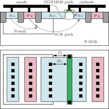
Figure 1 shows the cross-sectional view and the layout sketch of the proposed GGSCR structure. In this new structure, the drain (N+ bridge) of the gate structure is connected to the anode to form a new GGNMOS, which provides a new current path for triggering the low-voltage silicon-controlled rectifier (LVTSCR). When an ESD event occurs, the P-sub/N-drain PN junction of the GGNMOS avalanches first, and the electrons are injected from the source N+ region through the channel and then into the drain (N+ bridge). Meanwhile, the electrons in the N+ bridge will diffuse into the N-well due to the concentration difference between the N+ bridge and the N-well. As a result, there is a voltage drop across the parasitic resistor of the N-well, which in turn triggers on the SCR when the voltage drop is large enough.
 | Fig. 1. Cross-sectional view and layout sketch of the proposed GGSCR structure. |
In this investigation, the ESD transmission line pulse (TLP) measurements are carried out by using a pulsing signal with a rising time of 10 ns and a pulse width of 100 ns to emulate the human body model (HBM) of electrostatic discharge. The device is considered to be failed when its leakage current was increased by over three orders of magnitude under the TLP strike.
Figure 2 shows a comparison among the TLP characteristics of GGNMOS, conventional LVTSCR, and the proposed GGSCR. A double snapback behavior corresponding to the turn-on of GGNMOS and then SCR is observed. Before the second snapback, the ESD current is mainly released through the triggered GGNMOS. When the voltage drop across the parasitic resistance of the N-well reaches 0.7 V, the SCR will be turned on and thus provides a second path for conducting the ESD current. From the TLP results shown in Fig. 2, we can find that the holding voltage increases pronouncedly from 3.43 V to 6.25 V. This represents an 82% increase as compared with conventional LVTSCR and it does not consume any additional chip area.
 | Fig. 2. Comparisons of TLP characteristic among GGNMOS, LVTSCR, and GGSCR. |
The distance from N-well to channel (i.e., D1 shown in Fig. 1) is the key parameter for enhancing the holding voltage. Figure 3 shows the TLP test results of the proposed GGSCR as a function of D1. It can be seen that the trigger voltages are less sensitive to D1, but a larger D1 value can lead to a larger holding voltage. When D1 = 2 μ m, the holding voltage is 4.3 V, it increases up to 6.4 V when D1 is increased to 4.0 μ m.
 | Fig. 3. TLP results of GGSCR with different values of parameter D1. |
The ESD robustness is governed by the separation between the drain contact and gate boundary (D2 in Fig. 1). As shown in Fig. 4, when D2 is increased from 2.5 μ m to 4.5 μ m, the failure current (It2) increases from 2.48 A to 3.2 A. When the drain contact is close to the polysilicon gate (a small D2 value), the heat produced at the drain junction can be isotropically spread over the metal contact, and thus results in a lower level of failure current.[11] Thus, placing the contact farther away from the polysilicon gate can enhance the level of failure current. Another reason for increasing the level of failure current may be attributed to the drain ballast resistance in the embedded GGNMOS. The resistance increases as the distance of the contact to the polysilicon gate contact increases.
 | Fig. 4. TLP results of GGSCR with different values of parameter D2. |
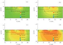
The underlying physical mechanism of the GGSCR can be explained with the aid of Sentaurus TCAD simulation. Figure 5 shows the TCAD simulated current density distribution of the GGSCR under different modes of operation. As shown in Fig. 5, the GGSCR passes through two different conduct phases as the pulsing current increases. The ESD current is mainly released by the GGNMOS (see Fig. 5(a)) before the SCR is triggered on. The conduction current may be small when the embedded GGNMOS just begins to bypass the current. Under this situation, the voltage drop across the substrate resistance may still not be large enough to trigger the SCR. As a result, as shown in Fig. 5(b), only a small portion of current passes through the SCR. As the current increases, although the current may still not large enough to trigger on the SCR, the current passing through the SCR increases to a level comparable to that through the GGNMOS (see Fig. 5(c)). Further increase of the GGMOS current will trigger on the SCR, thus causing a large current conduction via the SCR (see the bulk current in Fig. 5(d)).
 | Fig. 5. TCAD simulated current density profile of GGSCR under different operation modes. |
In this paper, we report an improved GGSCR for low-voltage ESD protection applications. TLP measurements on the GGSCR are made. Unlike GGNMOS nor LVTSCR, the proposed GGSCR demonstrates a dual snapback behavior and possesses a higher holding voltage due to the progressive turn-on sequence of parasitic GGNMOS and the SCR, which is confirmed with both experimental results and TCAD simulations. Better robustness of GGSCR is achieved by adjusting the spacing between the drain contact and gate boundary.
| 1 |
|
| 2 |
|
| 3 |
|
| 4 |
|
| 5 |
|
| 6 |
|
| 7 |
|
| 8 |
|
| 9 |
|
| 10 |
|
| 11 |
|