1.IntroductionThe bulk heterojunction (BHJ) organic solar cells (OSCs) have been intensively investigated in the past decade due to the advantages of being visibly transparent, compatible to flexible substrates, and light weight, etc.[1, 2] Such devices can be fabricated via a low-cost and high throughput process, a promising new-energy technology.[3– 6] The power conversion efficiencies (PCEs) of OSCs have reached over 10%, [7, 8] and the performances of the OSCs can be improved by sophisticated modification over the properties of photoactive materials, morphological control of the organic films, and electrical contact for charge collection by the electrodes.[9– 11]
The primary process of photocurrent generation is the generation of excitons after absorption of light. Then the excitons diffuse to the donor/acceptor interface and dissociate via ultrafast electron transfer into charge transfer (CT) states. In BHJ solar cells, the conversion of exciton-CT state has a quantum efficiency of almost unity. In order to generate a photocurrent, the bound CT states must dissociate into free electrons and holes and subsequently move to cathode and anode, respectively, before recombination processes take place. The loss and formation of CT states are believed to be key factors in determining the performances of the device. Two types of recombinations, i.e., the recombination of free carriers (non-geminate recombination) which forms CT states, and the recombination of CT states occurring at the donor/acceptor interface (geminate recombination), are closely related to the loss and formation of CT states. To understand the mechanisms behind the CT state process in BHJ solar cells, many researches of the two recombination processes have been performed.[12– 15] However, there is hardly any joint and comparative research about the influences of geminate and bimolecular recombination on the performances of OSCs.
The bimolecular recombination (Langevin recombination) and trap-assisted recombination (SRH recombination) are two different types of non-geminate recombinations. In most of OSCs, especially in the OSCs with high efficiency, the traps are so few that the bimolecular recombination dominates the non-geminate recombination.[13, 14] The influences of geminate recombination (GR) and bimolecular recombination (BR) on the performances of BHJ solar cells are studied in this article. And the losses in the OSCs are also studied. We find that a fraction of electrons (holes) in the device can be collected by anode (cathode). The direction of the corresponding current is opposite to the direction of photocurrent. This is another type of the CT state loss besides GR. The electrons (holes) collected by anode (cathode) are studied quantitatively for the first time. The performances of OSCs are improved largely if the electrons (holes) can be prevented from flowing out of the devices through anode (cathode).
Device simulation is an efficient way to study the interior working mechanism of OSCs.[16– 19] Here, the studies are performed through the device simulation method. Many factors, such as mobility, morphology, etc., could affect the GR or/and BR rate.[17] Therefore OSCs with different GR or BR rates could be fabricated by employing different materials or different preparation technologies.[17] However besides different GR and BR rates, when employing different materials or different preparation technologies, other characteristics such as the dissociation rate of CT states, absorption spectrum of the devices, etc., can be changed, which may also influence the performances of the devices. Through the simulation method, one can obtain some results which cannot be obtained experimentally.[18]
2.Numerical modelThe device is described by using the metal– insulator– metal picture. The BHJ layer is a mixture of donors and acceptors. It is considered as a homogeneous semiconductor. The energy difference between the lowest unoccupied molecular orbital (LUMO) of the acceptor and the highest occupied molecular orbital (HOMO) of the donor is considered to be an effective band gap (Egap) of the semiconductor. The thickness of the device is 100 nm. The rate of generation of CT states is assumed to be homogenous throughout the device. Though this is not to be strictly correct, it does not significantly influence the results and has been adopted by many researchers.[18– 20]
We employ a one-dimensional drift-diffusion model to calculate the charge generation and transport in the device.[18– 23] The electrostatic potential is calculated by Poisson equation

where x denotes the position within the device, q is the elementary charge, ɛ 0 is the vacuum dielectric constant, ɛ r is the relative dielectric constant, relating the potential Ψ (x) to the electron and hole densities n(x) and p(x), respectively. The charge carrier continuity equations are


where Jn(p)(x) is the electron (hole) current density, RB(x) denotes the BR rate of electron and hole, and kdiss(x)S(x) represents the generation rate of electrons and holes [see Eq. (11)]. The relevant current equations are


where Dn and Dp are the electron and hole diffusion coefficients respectively, μ n and μ p are the mobilities of electron and hole respectively, k is the Boltzmann’ s constant, and T is the absolute temperature. The cathode and anode are located at x = 0 and x = L respectively, where L is the device thickness. One assumption is that the semiconductor is always in thermodynamic equilibrium at the contact interface. The work functions of cathode and anode are assumed to line up with the conduction band and the valence band of the semiconductor respectively and the two contacts are both therefore Ohmic. Using Boltzmann statistics

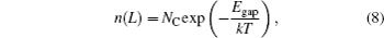


where NC(V) is the effective density of states of conduction (valence) band. The CT state continuity equation is given by

where S(x) is the concentration of the CT states and α is the coefficient of GR strength, α kf is the decay rate at which the CT state decays to a ground state, kdiss(x) is the dissociation rate of the charge transfer states, and GS(x) is the generation rate of the CT state. The dissociation rate of the CT states is described as


where J1 is the Bessel function of order one, where EB is the electron/hole pair binding energy, F(x) is the field strength, and a is the electron/hole pair distance of a CT state. The pair distance is described by a normalized distribution function
BR is expected to occur at the interface between the donor and acceptor in BHJ blends, with a rate


where β is the coefficient of BR strength. A device simulator ATLAS (Silvaco) is used for numerical simulations. All other parameters in the model used for computation are listed in Table 1.
Table 1.
Table 1.
 Table 1. Overview of the parameters used in the simulations. According to Eq. (13), the bonding energy of CT states (EB) is 0.236 eV.| Parameter | Symbol | Numerical value | Unit |
|---|
| Band gap | Egap | 1.0 | eV | | Electron mobility | μ n | 2.5× 10− 3 | cm2/V· s | | Hole mobility | μ p | 3× 10− 4 | cm2/V· s | | Efficient density of states | NC, NV | 2.5× 10¹⁹, 2.5× 10¹⁹ | cm− 3 | | Generation rate | GS | 1.8× 10²¹ | cm− 3 · s− 1 | | Relative dielectric constant | ɛ r | 3.4 | | | e/h pair distance | a | 1.8 | nm | | Decay rate | kf | 1.2× 10⁶ | s− 1 |
| Table 1. Overview of the parameters used in the simulations. According to Eq. (13), the bonding energy of CT states (EB) is 0.236 eV. |
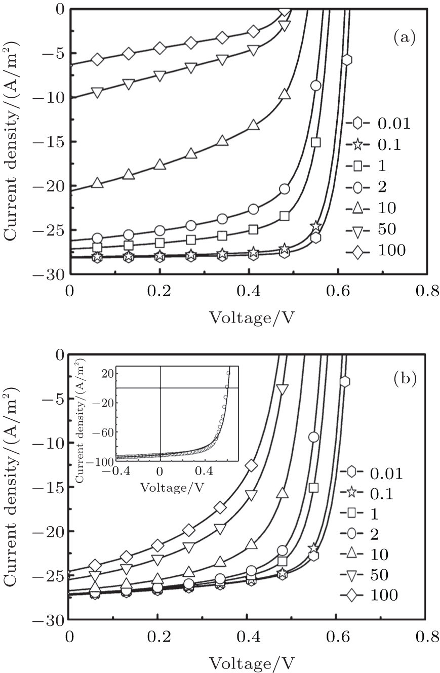
3.Results and discussionThe photovoltaic properties of the devices with different values of GR coefficient α and BR coefficient β are listed in Table 2 and the corresponding current density versus voltage (J– V) curves of these devices are shown in Figs. 1(a) and 1(b), respectively. According to Eq. (16), the BR intensity increases with β increasing. It is shown in Table 2 that as β increases, both the short circuit current density (JSC) and open circuit voltage (VOC) decrease. Experimentally, the BR intensity could be enhanced by various ways such as annealing which could increase the carrier mobility of the device.[17] However according to the work by Koster et al., the annealing, which also influences the dissociation rate of the CT states, actually increases rather than reduces JSC.[24]
Table 2.
Table 2.
Table 2. Solar cell characteristics.| α | β | JSC/(A/m2) | VOC/V | Wmax/(W/m2) | FF |
|---|
| 0.01 | | 28.14 | 0.63 | 14.26 | 80.93% | | 0.1 | | 28.05 | 0.62 | 13.75 | 79.65% | | 1 | 1 | 27.15 | 0.58 | 11.26 | 71.40% | | 2 | | 26.21 | 0.57 | 9.81 | 66.04% | | 10 | | 20.59 | 0.53 | 5.43 | 49.59% | | 50 | | 10.12 | 0.50 | 1.92 | 38.20% | | 100 | | 6.30 | 0.48 | 1.11 | 36.57% | | 0.01 | 27.22 | 0.62 | 12.61 | 74.29% | | 0.1 | 27.21 | 0.61 | 12.36 | 73.97% | | 1 | 27.15 | 0.58 | 11.26 | 71.40% | | 1 | 2 | 27.10 | 0.57 | 10.68 | 69.57% | | 10 | 26.73 | 0.53 | 8.88 | 62.68% | | 50 | 25.48 | 0.49 | 6.78 | 54.27% | | 100 | 24.54 | 0.47 | 5.90 | 50.84% |
| Table 2. Solar cell characteristics. |
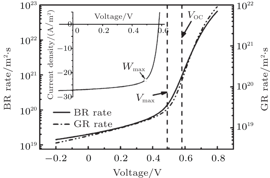
3.1.CT state losses in the OSCFigure 2 shows the variations of BR and the GR rate with bias voltage when α = 1/β = 1. And the inset displays the J– V characteristics. Both the BR rate and the GR rate increase with positive bias increasing. Especially at the voltage of Wmax, the BR rate and GR rate both begin to increase rapidly. Figure 3 shows a schematic diagram of the electronic process in the OSCs under operation condition. Since the conversion of exciton-CT state has a quantum efficiency of almost unity, the ratio of the CT states contributing to the photocurrent determines the performances of the OSC. The more the CT state losses, the smaller the photocurrent is. According to Fig. 3, the GR describes a loss process of the CT states (call GR loss hereafter). The faster the GR occurs, the more slowly the free carriers are generated. So the increase of GR rate induces the photocurrent to decrease. The positive bias would impede the transport of electron and hole to the cathode and anode, respectively. So the BR probability of the free carriers increases with positive bias increasing. The BR of free carriers would increase the concentration of CT states. According to Eq. (11), the GR rate is proportional to the concentration of the CT states, therefore the GR rate increases with positive voltage increasing.
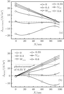
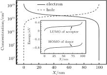
Figure 4 shows the hole and electron current densities in the device at different locations. Both the hole current at anode (JH, ANODE) and the electron current at cathode (JE, CATHODE) decrease as bias increases. When the bias is larger than VOC, the JH, ANODE and JE, CATHODE become negative. This means that the electrons and holes are injected into the device from the cathode and anode, respectively. And the directions of the corresponding currents are opposite to the direction of photocurrent, while the values of electron current at anode (JE, ANODE) and hole current at cathode (JH, CATHODE) are negative in the entire bias range. This means that the electrons and holes from active layer flow out of the device at anode and cathodes, respectively. The directions of the JE, ANODE and JH, CATHODE are opposite to the photocurrent. Therefore the total current, which is the sum of electron and hole current and constant throughout the device, is smaller than JH, ANODE or JE, CATHODE, (see Fig. 4(b), which shows that the photocurrent at a bias of 0.55 V is smaller than the corresponding JH, ANODE), JE, ANODE and JH, CATHODE counteract parts of JH, ANODE and JE, CATHODE, respectively. In other words, it is a form of CT state loss in OSCs (call current loss hereafter). This phenomenon has been observed by Koster et al., [19] but has not been investigated quantitatively yet. Furthermore, the JE, ANODE and JH, CATHODE increase with the bias increasing [see Fig. 4]. Consequently, the current loss increases [see Fig. 6]. It is worth noting that if the current loss can be prevented, the performances of the device must be largely improved. Figure 5 shows the electron and hole concentration profile at open circuit when α = 1/β = 1. The inset shows the corresponding energy levels. According to the energy levels, the electron should drift from the anode to cathode across the device. But the diffusion direction of the electrons is opposite to the drift direction due to the distribution of electron concentration in the device. In the vicinity of anode, the gradient of electron concentration is so large that the diffusion current of electrons is stronger than the drift current. Therefore the JE, ANODE is negative. The case of JH, CATHODE is similar.
Figure 6 shows the velocities of the electrons and holes flowing out of the device (VELETRON, VHOLE), the velocity of the GR of CT states in the device (VGR), the velocity of CT state loss caused by current loss (VCL), and the velocity of the CT state generation in the device (VG) at different bias voltages. The values VELETRON and VHOLE are equal. This is because the holes and electrons generate and recombine pairwise. According to Fig. 3, the photogenerated CT states vanish eventually by two ways: 1) relaxing to the ground through GR (GR loss); 2) flowing out of the device in the form of dissociated free electrons and holes (JE, CATHODE, JE, ANODE, JH, ANODE, and JH, CATHODE). Therefore, the sum of VGR and VELETRON (or VHOLE) is equal to VG. This means that there are two and only two types of CT state losses: GR loss and current loss. Furthermore under the condition of open circuit, the VCL is equal to VELETRON or VHOLE. This is because at VOC, the currents at anode and cathode are both 0. We can obtain VE, ANODE = VH, ANODE and VE, CATHODE = VH, CATHODE (VE, ANODE represents the velocity of electron flowing out the device from the cathode. VH, ANODE, VE, CATHODE, and VH, CATHODE are similar). We also have VCL = VH, CATHODE+ VE, ANODE, VELETRON = VE, ANODE+ VE, CATHODE, and VHOLE = VH, ANODE+ VH, CATHODE. Therefore, VCL = VELETRON and VCL = VHOLE can be obtained.
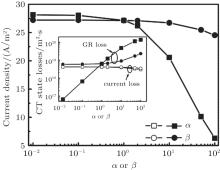
3.2.Short circuit currentThe values of JSC respectively as a function of α and β are plotted in Fig. 7. The GR coefficient α has a stronger influence on the JSC than β . The inset of Fig. 7 reveals the loss details of the CT state in the devices with different values of α and β respectively. With the increase of α or β , the current losses decrease while the GR losses increase. For the influence of α , when α < 0.6 the current loss dominates. Though the enhancement of GR loss is fast, the changing of current loss is slow, so the variation of JSC is small. When α > 0.6 the GR loss dominates. The short circuit current decreases sharply, since the GR loss increases rapidly with α increasing. For the influence of β , the GR loss dominates in the entire range. For α = 100/β = 1, the GR rate is about 21 times the value for the case of α = 1/β = 1. While for α = 1/β = 100, the GR rate is about 3.8 times the value in the case of α = 1/β = 1. The GR loss influenced by α is larger than β , therefore α has a stronger influence on the JSC than β .
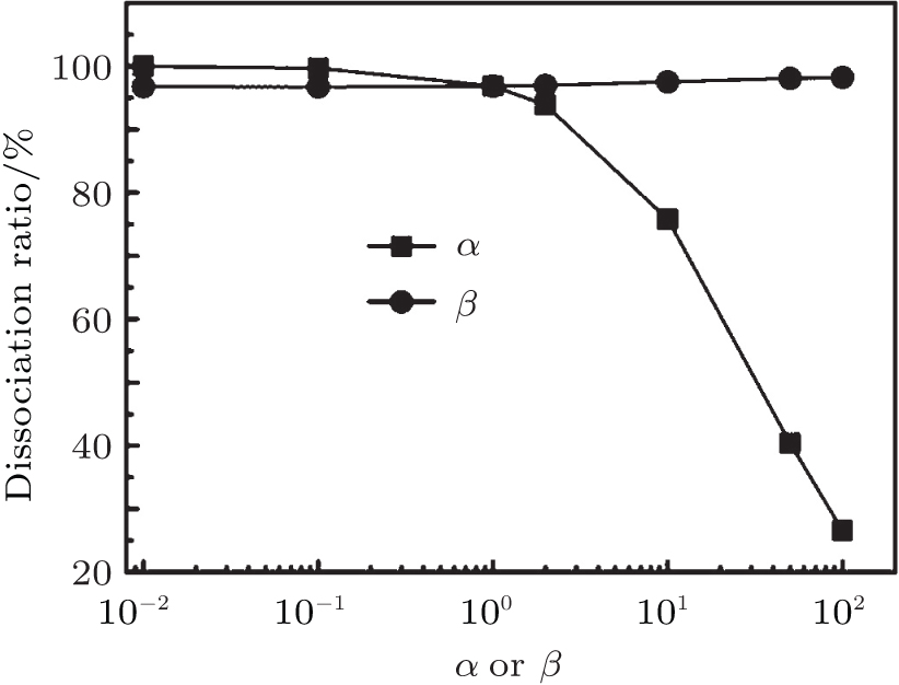
To investigate the GR loss influenced by α and β , we calculate the average dissociation ratio of bound CT states. The results are shown in Fig. 8. With the increase of α , the dissociation ratio decreases rapidly. While with the increase of β , the dissociation ratio almost remain unchanged or even increases slowly. Therefore GR loss influenced by α is larger than that by β .
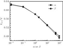
3.3.Open circuit voltageThe values of VOC relatively as a function of α and β are plotted in Fig. 9. VOC values decrease respectively with α and β increasing. Moreover it is interesting that the VOC values influenced by α and β are about the same. In Ref. [26], the VOC obtained by authors is given by

where γ is the BR constant and can be represented by β rL, and P is the dissociation ratio of the CT states. The value of VOC obtained by the formula is in good agreement with the corresponding experimental value. Using Eq. (18) one can further have

It is clear that α and β play the same role in the formula. Therefore the variations of VOC, influenced by α and β , are almost the same. In Ref. [26] the relation of VOC∼ ln(GS) is linear. However the relations of VOC∼ ln(α ) and VOC∼ ln(β ) are not linear here, especially when α or β is less than 1. That is because the dissociation rate of the CT state kdiss is fielddependent. When α or β changes, the concentration of charge carriers will change. According to Eq. (1) the electrostatic potential and electrical field will change with the concentration of charge carriers.
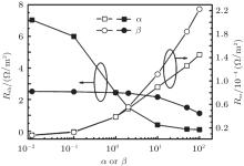
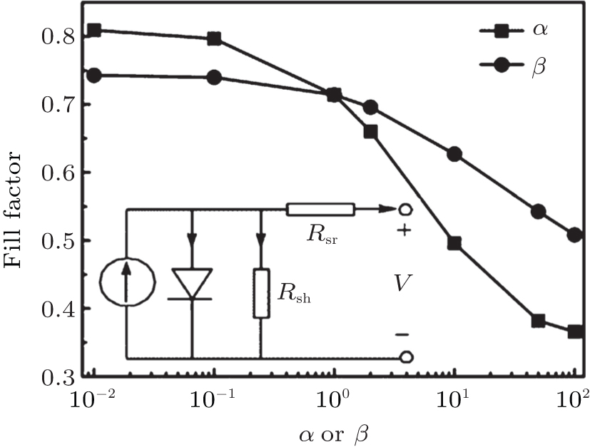
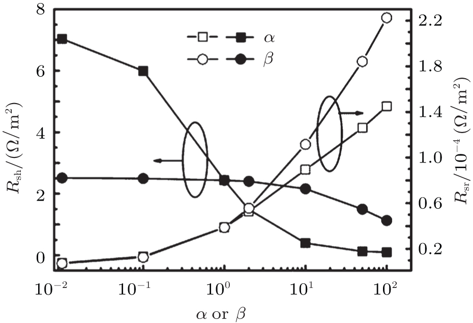
3.4.Fill factorFigure 10 shows the fill factor (FF) values of the OSCs respectively as a function of α and β . The FF values decrease respectively with α and β increasing, and the influence of α is stronger than that of β . We consider the equivalent circuit of the OSC illustrated in the inset of Fig. 10. Both the larger series resistance (Rsr) and the smaller shunt resistance (Rsh) result in a lower FF.[27, 28] As shown in Fig. 11, Rsr increases and Rsh decreases with α and β increasing. α influences Rsh more than β , but α influences Rsr less than β .
Rsr induces a voltage drop on itself, it can separate the applied voltage from the diode. The larger the Rsr, the less the voltage drop on the diode is, which results in a slower increase of J with V rising, accordingly the less “ square” the J– V curve becomes.[30, 31] Generally Rsr is composed of (i) bulk resistance of the organic layer, (ii) bulk resistance of the electrodes, (iii) contact resistance of each interface in the device, and (iv) probe resistance. Since it is the numerical simulation here and the contacts of anode and cathode are Ohmic contacts, the resistances mentioned in items (ii)– (iv) are negligible.[28] The buildup of space charge should not play a role here. Space charges in BHJ solar cells are caused by a large difference in mobility between electrons and holes with a high illumination intensity.[32] While the mobility difference in this study is small (smaller than one order). If the space charge limited photocurrent plays a role, the FF should smaller than 42%.[32] Therefore the bulk resistance can be expressed as:[28]

Here, A is the cross-sectional area and L is the thickness of the device. We can see that the concentrations of hole and electrons determine the series resistance of the OSC. The hole and electron concentration of the OSCs at open circuit are shown in Fig. 11. As α or β increases, the electron and hole concentrations both decrease, which is related to the increase of Rsr. Moreover, the concentrations of electrons and holes are influenced more strongly by β than by α . Thus α influences Rsr less than β .
Shunt resistance represents the current leakage in the cells. It has the effect of separating the current in the equivalent circuit. Ideal Rsh should approach to infinity, so current flowing through Rsh is zero, i.e., there exists no current leakage in the device. The current will not change with the applied voltage at 0 or reverse bias. If Rsh is small, the current flowing through it cannot be neglected. The current will change with the applied voltage at 0 or reverse bias, which makes the J– V curve deviate from “ square” , thus leading to a lower FF. In the equivalent circuit, the shunt resistance under illumination (Rsh) can be divided into two parts: one describes the shunt resistance in the dark (RshD), attributed to device pinholes and current leakage, and the other handles CT state dissociation (RshCT), and they are related by the following expression:[33]

According to the discussion in the previous sections, GR rate increases with α or β . And GR rate influenced by α is larger than by β . The larger the GR rate in the device, the smaller the RshCT is, which results in a smaller Rsh.


 , Qi Ling-Hui, Du Hui-Jing‡