Temperature-dependent photoluminescence spectra of GaN epitaxial layer grown on Si (111) substrate
State Key Laboratory on Integrated Optoelectronics, Institute of Semiconductors, Chinese Academy of Sciences, Beijing 100083, China
†Corresponding author. E-mail: dgzhao@red.semi.ac.cn
*Project supported by the National Natural Science Foundation of China (Grant Nos. 61474110, 61377020, 61376089, 61223005, and 61176126) and the National Science Fund for Distinguished Young Scholars of China (Grant No. 60925017).
1.IntroductionThe III-nitrides have attracted much attention due to their multiple applications in ultra-violet (UV) blue light-emitting diodes, high frequency electronics, optoelectronics, and high power electronics.[1– 4] Owing to a lack of a commercial homosubstrate, the growth of GaN has been generally developed on foreign substrates, such as sapphire[5] and silicon.[6, 7] With the improvement of material growth and processing technology, the crystalline quality of GaN epitaxial layer usually becomes quite good. It is necessary to further understand the basic properties of GaN epitaxial layers, especially those that are grown on desired silicon wafers. The optical properties, especially the photoluminescence (PL) of GaN have received much attention.
The fundamental optical transitions in GaN, including the binding energies of the free excitons (FXs) associated with different valence bands, have been clarified by Chen et al.[8] Paskova et al. observed a dominating donor– acceptor pair DAP emission at about 3.27 eV.[9] Liu et al. has reported that the presence of stacking faults results in luminescence peaks ranging from 3.29 eV to 3.41 eV.[10] However, there are still few reports that have focused on the photoluminescence studies of GaN grown on Si (111).
In this paper, the optical properties of GaN films grown on Si (111) are studied. To further understand the influence of stress on the photoluminescence of GaN grown on Si (111), GaN epitaxial layers grown on sapphire substrates are also investigated.
2.ExperimentThe samples are grown by metal-organic chemical vapor deposition (MOCVD). Trimethylgallium (TMGa), trimethylaluminum (TMAl), and ammonia (NH3) are used as Ga, Al, and N precursors, respectively. Samples with different substrates are grown. Samples A and B are grown on Si (111) substrates at different growth temperatures. The buffer layers are AlN and AlGaN, followed by GaN epitaxial layer. The thickness values of epitaxial layers of sample A and sample B are 0.9 μ m and 2.5 μ m, respectively. The full widths at half maximum (FWHMs) of x-ray diffraction (XRD) of GaN on (0002) plane of samples A and B are 780 arcsec and 320 arcsec, respectively. Sample C is grown on c-plane sapphire for a comparison, and the epitaxial layer is 1.5 μ m. Raman spectra and photoluminescence (PL) are measured to investigate the optical properties of GaN epitaxial layers. The Raman spectra have been recorded at room temperature and the He– Ne laser (632.8 nm) is used for the excitation. The temperature-dependent PL measurements are carried out using He– Cd laser operating at 325 nm as an excitation source and the spectral resolution is < 0.1 meV for the whole energy range.
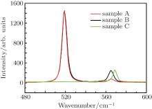
3.Results and discussionThe Raman spectra of all samples are measured at room temperature to check the stress conditions of the samples. The measured Raman spectra of all of the samples are presented in Fig. 1. The nominal E2 phonon peak frequency of the relaxed GaN bulk material[11] is 567.6 cm− 1. The increase of the E2 peak frequency is due to a compressive strain in the film, while the decrease in E2 mode frequency is attributed to tensile stress.[12] Because the thermal mismatch and the lattice mismatch between GaN and different substrates are different, it is understood that GaN films grown on different substrates exhibit different stress conditions. For sample C, the E2 mode is found to be at 568.8 cm− 1, which corresponds to a compressive strain of 2.1 GPa according to a stress coefficient of 4.3 cm− 1/GPa for GaN.[13] However, for samples A and B, the E2 modes are observed at 565.5 cm− 1 and 565.0 cm− 1, lower than 567.6 cm− 1, corresponding to tensile strains of 3.6 GPa and 4.6 GPa. Therefore, GaN films grown on different substrates display different stress conditions. Actually, even when grown on the same substrate, the stress condition of GaN films may also be different from each other, depending on their different growth conditions.
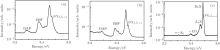
Figure 2 presents the PL spectra of samples A and B measured at 8 K. For sample A, there are two peaks located, respectively, at 3.458 eV and 3.475 eV close to the band gap edge of hexagonal GaN at low temperature. They have an energy separation of 17 meV. It is well known that the energy difference between two exciton luminescence peaks, i.e., D0X and (FXA)n= 1, is much smaller, normally 6 meV– 9 meV.[8, 14] So these two peaks are not assigned to D0X and (FXA)n= 1. The FWHM of the peak located at 3.458 eV is 13.4 meV. Actually, the FWHM of this peak is quite large, so we deem it to be formed by two unresolved peaks of D0X and (FXA)n= 1. We think that the peak position located at 3.458 eV is mainly determined by (FXA)n= 1, and peak position located at 3.475 eV is attributed to (FXA)n= 2. Based on the energy difference between the two peaks (FXA)n= 1 and (FXA)n= 2, i.e., the ground and excited states of A-exciton, and using a simple hydrogen-like model which neglects small anisotropy, the binding energy of A-exciton can be calculated to be 22 meV (4/3 × 17 meV). This value is in agreement with that reported in Ref. [14]. Furthermore, there are two additional peaks located at the position lower than the band gap energy. One is a broad emission peak at 3.377 eV, which may be attributed to stacking faults (SFs), [10] and another peak at 3.286 eV is due to donor– acceptor-pair (DAP) luminescence.[9] The main emission peaks for sample B are similar to those for sample A, but have some small shifts of the peak positions. The peak located at 3.466 eV is attributed to the merged D0X and (FXA)n= 1, and its FWHM is 10.4 meV. This value is a little smaller than that of sample A, implying that the crystal quality of sample B is higher than that of sample A. The peak of (FXA)n= 2 is found to be located at 3.483 eV, and the emission peak at 3.387 eV with a shoulder is attributed to SFs in a similar way to that for sample A.[10, 15, 16] We make a comparison of photoluminescence property between sample A and sample B. The photoluminescence efficiency of sample A is about 4.4%, while that of sample B is as high as 39.5%. Furthermore, the room-temperature PL intensity of sample B is stronger than that of sample A. These results are attributed to the fact that the crystal quality of sample B is higher than sample A.
For sample C, which is grown on sapphire, the D0X and FXA peaks are well resolved at 8 K, and are located at 3.491 eV and 3.497 eV, respectively. This is in good agreement with what was reported in the literature for GaN films grown on sapphire.[17] At the same time, there are a neutral acceptor-bound exciton (A0X) transition peak, and two longitudinal optical (LO) phonon replicas of FXA and D0X, separated by 90 meV between the FXA and D0X peaks, as well as a band-to-acceptor (e-A0) transition located in 3.308 eV. No SF-related peaks are observed. This indicates that the density of SF defects in the GaN film grown on sapphire is usually much lower than that grown on Si (111).
According to the above-mentioned results, the positions of D0X and (FXA)n= 1 peaks for GaN films grown on Si (111) substrates undergo red shifts compared with those grown on sapphire. This is mainly due to the fact that the GaN films grown on Si (111) substrate are under action of tensile stress, while those grown on sapphire are subjected to compressive stress, [13] which is clearly shown by our measurements of Raman spectra. In fact, the D0X peak for strain-relaxed GaN film is located at 3.471 eV.[18] This implies that the deviations of peak position induced by tensile stress and compressive stress should be opposite to each other in direction. Furthermore, because the stress conditions of sample A and sample B are slightly different from each other, even though both of them are grown on an Si (111) substrate, their excitonic luminescence peaks also shift a little relatively due to different stress conditions caused by different growth parameters of these two samples.
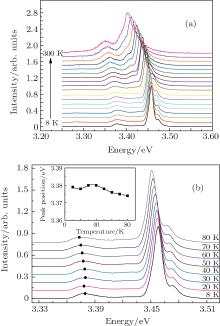
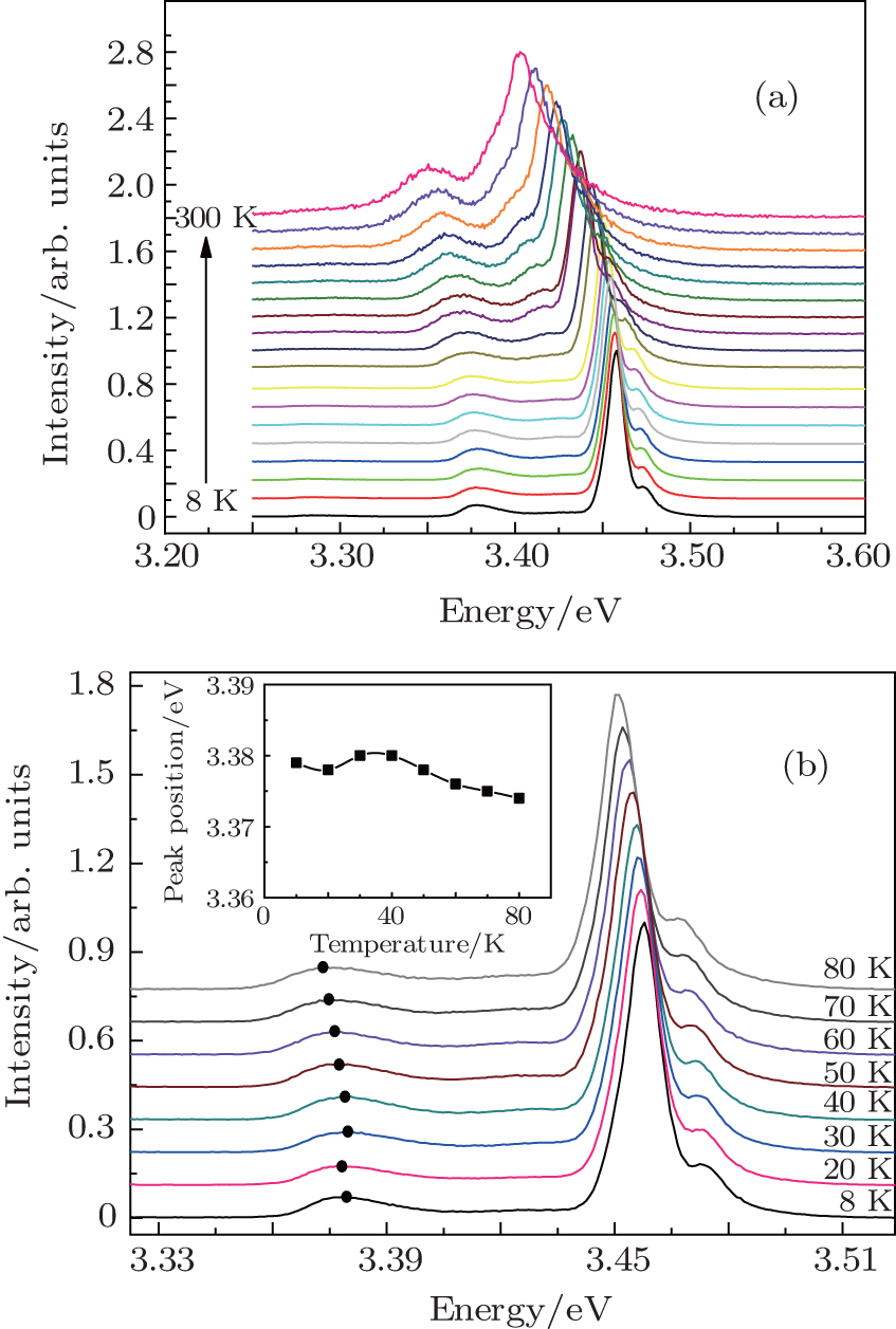
To further study the emission peaks caused by SFs, we investigate the temperature dependence of PL spectra of sample A. Figure 3(a) shows PL spectra ranging from 8 K to 300 K and figure 3(b) displays the spectra of Fig. 3(a) with a magnified photon energy scale ranging from 8 K to 80 K. The black dots in Fig. 3(b) represent the temperature-dependent peak positions of SFs and the inset of Fig. 3(b) shows the relationship between the peak position of SFs and temperature. As shown in Fig. 3(a), each of the PL peaks of excitonic recombination undergoes a redshift with increasing temperature due to the thermally induced band-gap shrinkage. At room temperature, the excitonic recombination peaks ((FXA)n= 1, D0X, and (FXA)n= 2) merge into a broad luminescence peak while the peak caused by SFs can still be resolved clearly. In Fig. 3(b) no S-type temperature behavior can be well distinguished from the PL peak of (FXA)n= 1 and D0X in the temperature range between 8 K and 80 K. However, it is interesting to note that the SFs peak exhibits a clear behavior of S-type dependence. In the temperature range 8 K– 40 K, the position of peak caused by SFs first undergoes a slight red shift, and then a blue shift, and above 40 K the peak indicates a red shift with increasing temperature.
It is known that at SFs the hetero-structural domains will form due to the fact that there are two different GaN crystal structures, i.e., hexagonal wurtzite and cubic zinc-blende, on the two sides of the domain boundary. The wurtzite structure corresponds to a larger energy gap while the zinc-blende structure has a narrower band gap. Therefore, SFs in GaN can introduce a kind of quantum well, where thin zinc-blende region is embedded in the wurtzite matrix, [19] thus the SFsrelated luminescence may correspond to the QW emission.[20] We think that the SFs emission occurs from a bundle of SFsrather than from a single one. SFs can be regarded as many quantum wells which could have different QW widths. The localized states can be induced by the fluctuation of well thickness. The observed S-type temperature-dependent behavior of the SFs luminescence peak may be attributed to the influence of the QW emission by the localized states near the conduction band edge and the temperature-dependent distribution of the photo-generated carriers.
4.ConclusionsThe optical properties of GaN films grown on Si (111) are studied. The main emission peaks of GaN films grown on Si (111) are identified. The positions of D0X and FXA peaks for GaN films grown on Si (111) each undergo a red shift compared with those grown on sapphire. This is attributed to the fact that GaN film grown on sapphire is under action of compressive stress, while GaN film grown on Si (111) substrate is subjected to tensile stress. The emission peaks attributed to stacking faults are identified. S-shaped temperature dependence of PL spectra can be observed, owing to the influence of the QW emission by the localized states near the conduction band edge and the temperature-dependent distribution of the photo-generated carriers.


 , Jiang De-Sheng, Liu Zong-Shun, Zhu Jian-Jun, Chen Ping, Liu Wei, Li Xiang, Shi Ming]