C–H complex defects and their influence in ZnO single crystal
[Xie Hui, Zhao You-Wen† , Liu Tong, Dong Zhi-Yuan, Yang Jun, Liu Jing-Ming]
, Liu Tong, Dong Zhi-Yuan, Yang Jun, Liu Jing-Ming]
|
|


†Corresponding author. E-mail: zhaoyw@semi.ac.cn
*Project supported by the National Natural Science Foundation of China (Grant No. 61474104).
Infrared absorption local vibration mode (LVM) spectroscopy is used to study hydrogen related defects in n-type ZnO single crystal grown by a closed chemical vapor transport (CVT) method under Zn-rich growth conditions, in which carbon is used as a transport agent. Two C–H complex related absorption peaks at 2850 cm−1 and 2919 cm−1 are detected in the sample. The formation of the C–H complex implies an effect of carbon donor passivation and formation suppression of H donor in ZnO. The influence of the complex defects on the electrical property of the CVT-ZnO is discussed based on Hall measurement results and residual impurity analysis.
Zinc oxide (ZnO) is a wide band gap semiconductor that has been studied widely due to its potential application in ultraviolet (UV) optoelectronic devices.[1] However, high concentrations of native defects and impurities, such as oxygen vacancy, hydrogen etc., are easily formed or incorporated into the growth process of ZnO material.[2– 4] These defects and impurities always make ZnO materials exhibit n-type conduction. Meanwhile, a stable p-type material is quite difficult to obtain. The results of recent research demonstrate that H acts as a shallow donor and many H related complex defects have been detected in ZnO grown by hydrothermal (HT) method or treated by H plasma.[5– 8] It is necessary to study the formation of the hydrogen complex defects under different growth conditions, as well as their thermal stabilities and influence on the electrical properties of a ZnO single crystal.
In the present work, we present the infrared absorption results of an n-type ZnO single crystal that is grown by a closed chemical vapor transport (CVT) method under Zn-rich growth condition, in which carbon is used as a transport agent. The results suggest that C– H complex is formed in the growth process of the ZnO single crystal. By comparing our results with the reported results of HT-ZnO samples, it is believed that the formation of this complex defect is correlated with the Zn-rich growth condition and high concentration of carbon involved in the growth process. As expected, the electrical measurement results indicate that the carbon donor is passivated by this complex defect and it is activated after high temperature annealing.
ZnO single crystal samples were grown by a closed seeded chemical vapor transport method in which carbon was used as a transport agent.[9] The growth took place under a Zn-rich condition since the carbon transport agent consumed oxygen in the growth process. A single crystal ZnO wafer, whose two sides had been polished, with a size of 5 mm × 5 mm × 0.5 mm was used for the infrared absorption local vibration mode (LVM) measurement. The Hall effect was measured by a conventional van der Pauw method through using indium ohmic contact. The impurity content in the ZnO sample was checked by glow discharge mass spectroscopy (GDMS) measurement.
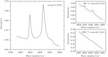
Figure 1 shows the infrared absorption LVM spectra of a ZnO single crystal sample grown by the CVT method. Two absorption peaks located, respectively, at wave numbers of 2850 cm− 1 and 2919 cm− 1 can be observed in the spectrum. According to the wave number of hydrogen related LVM in a number of semiconductors reported in the literature, the relationship between the mass of the complex defect and its vibration frequency is described as
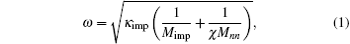
where ω is the frequency of the vibrational mode, kimp is the force constant between the atom and its neighbor, χ is the parameter that depends on the local angle bending and bond stretching force constant, Mimp is the mass of the impurity atom, and Mnn is the mass of the atom adjacent to the impurity.[10] It is easy to figure out that the observed LVM is related to the C– H complex defect.[11– 14] Nickel and Fleischer reported a number of C– H related LVMs in a range of 2800 cm− 1– 3000 cm− 1 by Raman scattering in chemical vapor grown ZnO single crystal samples.[15] The vibrational modes located at 2854 cm− 1 and 2918 cm− 1 were assigned to be the stretching mode of C– H and symmetric stretching mode of C– H2, respectively. Thus, this result implies the formation of C– H complex defect in the growth process of ZnO single crystal via the CVT method. It is noted that hydrothermal (HT) method grown or hydrogen plasma treated ZnO single crystal contains a number of O– H related LVMs in a range of 3300 cm− 1– 3600 cm− 1, [16– 20] while such an LVM is not detected in our ZnO single crystal samples. This phenomenon is most likely to be related to the difference in growth condition between the CVT and HT; i.e., the difference between Zn-rich condition and O-rich condition. Since carbon is used as the transport agent in the process of the closed CVT growth, the transport related chemical reactions are as follows:


It is apparent that the transport is realized through a consumption of oxygen by carbon in the growth process of the closed CVT and the Zn-rich growth condition cannot be avoided for the ZnO single crystal. Naturally, the high concentration of oxygen vacancy is easily formed in this case. As for the hydrogen, it usually originates from residual water in the ZnO source material.
Since oxygen vacancy is the dominant native defect in the CVT ZnO single crystal grown under Zn-rich growth condition, it will inhibit the formation of an O– H related complex defect. In contrast, a Zn vacancy is a dominant defect in a HT grown ZnO single crystal which is grown under O rich conditions.[21, 22] It is natural that O– H complex is easily formed without the involvement of carbon in the HT growth process.
As for the composition of the two complex defects, the two LVM peaks are likely to originate from the C– H complex. Generally, the vibrational frequency ratio has the following relationship:[12, 23, 24]

where ω 1 and ω 2 are the C– H and C– H2 frequencies, respectively; and, M1 and M2 are the molar mass values of the C– H and C– H2 complexes, respectively. The vibrational frequency ratio is r = ω 1/ω 2 = 1.024, which is very close to the square root of their mass ration (r = 1.037). This gives further support that the absorption peaks at 2850 cm− 1 and 2919 cm− 1 are characteristics of C– H in CVT-ZnO. Thus, it is reasonable that the stretch modes of C– H2 and C– H complexes have frequencies of 2850 cm− 1 and 2919 cm− 1, respectively (as shown in Fig. 1).
It has been reported that C is a donor in ZnO single crystal, with the donor level being at 310 meV below the conduction band and a characteristic photoluminescence emission being at 3.06 eV.[25] It has also been confirmed that H is a shallow donor defect in ZnO.[26, 27] Since hydrogen has a passivation effect by forming a complex defect in semiconductors, it is necessary to study the variations of the electrical property of the CVT-ZnO single crystal in as-grown and annealed state, corresponding to the situation of the formation and the dissociation of the complex defect in the material.
 | Fig. 1. Infrared absorption LVM spectra of a ZnO single crystal sample grown by CVT method, without and with annealing. |
After the ZnO sample is annealed at 1000 ° C for 2 h in O2, there is no detected absorption peak in a wave number range of 2800 cm− 1– 3000 cm− 1, as shown in Fig. 1. But there are still the two absorption peaks in ZnO after being annealed at 800 ° C. This indicates that the C– H complexes are decomposed after being annealed at a high temperature (1000 ° C). Since H is easily removed through outdiffusion in the annealing process, it is proposed that the carbon atom has a tendency to occupy the Zn sites and generate a donor defect. The processes of the decomposition and substitution are as follows:


In addition, native defects in ZnO, such as oxygen vacancy or zinc interstitial, are easily suppressed after high temperature annealing. This phenomenon is widely confirmed by the thermally induced disappearance of oxygen vacancy related photoluminescence green band, which is attributed to the transition from the deep level defects, such as oxygen vacancy or zinc interstitial in ZnO.[28] A recently reported result also suggested that the concentration of oxygen vacancies in ZnO was reduced after high temperature annealing.[29] The deep level transient result of our annealed ZnO sample indicates a basically full suppression of the deep level defects in the as-grown ZnO.[30] Thus, the influence of the deep level native defects on the property of the annealed ZnO is negligible.
Our Hall measurement results are given in Table 1. It is apparent that the carrier concentration of the ntype ZnO single crystal sample increases after the annealing treatment. This phenomenon suggests that donor defect is formed in the material after the annealing treatment. Furthermore, the impurity content is quite low, especially the common donors Ga, In, and Al in the ZnO sample have a slight decrease after annealing.
| Table 1. Hall measurement results of ZnO samples. |
Thus, it is believed that the thermally induced carrier concentration increase is caused by the thermal decomposition of the C– H complex defect. The decompositions of the C– H complex defects lead to the activation of a portion of C donors, even if H donors are not considered. This makes the annealed ZnO single crystal exhibit a higher carrier concentration.
By combining the experimental results, the formation of the C– H complex defect gives a passivation effect of the C donor and suppression formation of the H donor defect in the CVT-ZnO single crystal. This is most likely to be a reason why the high quality n-type ZnO single crystal with low carrier concentration and high mobility can be grown even if it is contaminated by carbon in the growth process of the closed CVT.
C– H complex defects are formed in ZnO single crystal grown by the closed CVT method in which carbon is used as a transport agent. The formation of the complex defect has an effect of carbon donor passivation. The carrier concentration of the n-type ZnO single crystal increases with the thermal decomposition of the complex.
| 1 |
|
| 2 |
|
| 3 |
|
| 4 |
|
| 5 |
|
| 6 |
|
| 7 |
|
| 8 |
|
| 9 |
|
| 10 |
|
| 11 |
|
| 12 |
|
| 13 |
|
| 14 |
|
| 15 |
|
| 16 |
|
| 17 |
|
| 18 |
|
| 19 |
|
| 20 |
|
| 21 |
|
| 22 |
|
| 23 |
|
| 24 |
|
| 25 |
|
| 26 |
|
| 27 |
|
| 28 |
|
| 29 |
|
| 30 |
|