Li Xue-Dong, Liu Hong, Wu Jia-Gang, Liu Gang, Xiao Ding-Quan, Zhu Jian-Guo†. The interface density dependence of the electrical properties of 0.9Pb(Sc0.5Ta0.5)O3–0.1PbTiO3/0.55Pb(Sc0.5Ta0.5)O3–0.45PbTiO3 multilayer thin films . Chinese Physics B, 24(10): 107701
Permissions
The interface density dependence of the electrical properties of 0.9Pb(Sc0.5Ta0.5)O3–0.1PbTiO3/0.55Pb(Sc0.5Ta0.5)O3–0.45PbTiO3 multilayer thin films
Li Xue-Donga),b), Liu Hongb), Wu Jia-Gangb), Liu Ganga), Xiao Ding-Quanb), Zhu Jian-Guo†b)
College of Physics and Electric Engineering, Mianyang Normal University, Mianyang 621000, China
College of Materials Science and Engineering, Sichuan University, Chengdu 610064, China
*Project supported by the National Natural Science Foundation of China (Grant No. 60771016) and the Scientific Research Foundation of Mianyang Normal University, China (Grant No. QD2013A07).
Abstract
The 0.9Pb(Sc0.5Ta0.5)O3–0.1PbTiO3/0.55Pb(Sc0.5Ta0.5)O3–0.45PbTiO3 multilayer thin films ((PSTT10/45) n, n = 1–6, 10) are deposited on SiO2/Si(100) substrates by radio frequency magnetron sputtering technique with LaNiO3 buffer and electrode layer, and the films are subsequently annealed by a two-step rapid thermal approach. It is found that the interfacial density of the film has an important influence on the electric property of the film. The electric property of the film increases and reaches its critical point with the increase of interface density, and then decreases with the further increase of the interface density. With an interfacial density of 16 μm−1, the film shows an optimized dielectric property (high dielectric constant, εr = 765, lowest dielectric loss, tan δ = 0.041, at 1 kHz) and ferroelectric property (highest remnant polarization, 2 Pr = 36.9 μC/cm2, low coercive field, 2 Ec = 71.9 kV/cm). The possible reason for the electric behavior of the film is the competition of the interface stress with the interface defect.
PACS:
77.55.fp; 77.22.–d; 77.80.bn
Keyword:
ferroelectric multilayer thin films; electrical properties; interface density
Ferroelectric thin films have attracted much attention in recent years because of their practical or potential applications in various fields, such as ferroelectric nonvolatile random access memories, modulators, ferroelectric photovoltaic devices, etc.[1– 3] Among this research, Pb(Sc0.5Ta0.5)O3 (PST) has been one of the most extensively studied materials for uncooled infrared radiation sensor applications due to its excellent pyroelectric properties and high figures of merit.[4– 6] However, the Curie temperature (TC) of PST is between 0 and 25 ° C, which often restricts its application. To modify the features of the ferroelectrics, three methods are often used in preparation: doping, [7, 8] substitution, [9] and solid solution.[10, 11] Mixing PST with lead titanate (PbTiO3, PT), e.g., (1 − x) Pb(Sc0.5Ta0.5)O3– xPbTiO3, PSTTx, is an effective way to raise the TC, and then the high pyroelectric property could be retained.[6, 12]
Another attractive material is multilayer thin film. As is well known, the coupling and interaction between the layers in a multilayer structure can strongly affect the film’ s electrical properties, [13– 15] and an appropriate combination of the layers with different compositions can either improve the functional properties or create one or more novel properties.[16, 17] Inside multilayer thin film, interfacial intensity[18] or periodicity[19, 20] can greatly influence the electrical performance of the film.
In our previous work, various efforts have been made to improve the properties of PSTT single films, including the heat treatment of common rapid thermal annealing (RTA), [21] a novel two-step rapid thermal annealing (TSRTA) which can greatly reduce the duration of the film retained in high temperature, [22– 24] preparing Pb(Zr0.52, Ti0.48)O3 (PZT52/48) as a seed layer, [25] and fabricating a composition differential multilayer thin film (PSTT10/45).[26] Recently, epitaxial PST films with good ferroelectric properties were also grown on electroded and buffered Si (100) substrates.[27]
In the present work, (PSTT10/45)n (n = 1– 6, 10) multilayer thin films are deposited on Si (100) substrates by radio frequency (RF) magnetron sputtering. The total thickness values of PSTT10 and PSTT45 are kept unchanged, respectively. The influences of interface density on electrical properties of the films are investigated, and the physical mechanisms for enhancing the electrical properties are also discussed.
2. Experiment
PSTT10, PSTT45, and LNO were all made into powder targets by conventional mixed-oxide processing. The LNO buffer layer with a thickness of about 550 nm was deposited on an SiO2/Si (100) substrate by RF magnetron sputtering (JGP5600, SKY Co., China), and then the sample was annealed at 750 ° C for 1.5 min in a RTA furnace (Mila-3000, ULVAC-RIKO, Japan) to pre-crystallize LNO seed layer. The 1– 6 and 10 periodicities of PSTT10/45 ferroelectric multilayer thin films with a cap layer of PSTT10 were deposited on LNO/SiO2/Si (100) substrate at 350 ° C by RF magnetron sputtering, whose detailed structure information was given in the previous work.[26] Total thickness values of PSTT10 and PSTT45 films were both 250 nm. The films were then post-deposition annealed three times by the TSRTA method[22– 24] with a peak temperature of 750 ° C and a maintaining temperature of 450 ° C. Sputtering and annealing details were referred from the previous work.[21– 24] The number of interfaces per micrometer Ni/d, with Ni being the number of interfaces (Ni = 2n) and d the film thickness, is introduced as a measure of the interface density.
The crystalline phases of the films were identified by x-ray diffraction (XRD) (DX-1000, Dandong, China). The microstructures of the films were analyzed by scanning electron microscope (Inspect F, FEI Company, Netherlands). In order to measure the ferroelectric properties of the films, dot-type gold electrodes with an area of 2 × 10− 3 cm2 were deposited by direct current sputtering, which formed stacked capacitors. The polarization electric field (P– E) hysteresis loops and the leakage current behaviors were measured using radiant precision ferroelectric measurement system (RT2000 Tester, USA).
3. Results
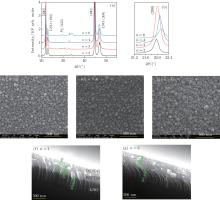
Figure 1(a) shows XRD patterns of the (PSTT10/45)n multilayer thin films. All (PSTT10/45)n multilayer thin films possess highly (100) orientation with little second phase, as indicated unusually by high-intensity (200) and (400) peaks. The LNO buffer layer is introduced to reduce the lattice and thermal mismatch, and the physical mechanism for the (100) orientation of the films was discussed elsewhere.[22, 26] Figure 1(b) shows the expanded XRD patterns of the (200) peaks of the multilayer thin films. It is found that the positions of the (200) peaks of the films are shifted to higher angles with the increase of n. So it is thought that the lattice distortion happens in the (PSTT10/45)n multilayer thin films. Surface morphologies of the (PSTT10/45)n thin films with n = 2, 4, 6 are shown in Figs. 1(c)– 1(e). All of the samples demonstrate uniform crystal sizes and cavity free surfaces. The surfaces of three samples are very similar to each other, revealing that the surface morphology is not a key factor to the properties of the multilayer thin films. Cross section images of the (PSTT10/45)n thin films with n = 1, 2 are shown in Figs. 1(f) and 1(g). In Fig. 1(f) clear demarcations can be seen between LNO, PSTT10, and PSTT45. In Fig. 1(g) a clear demarcation can be seen at the LNO/PSTT10 interface and a rough demarcation can be seen in the PSTT10/45 segment. The columnar growths of LNO and PSTT can be seen from the two images, confirming the well and oriented growths of the films. A similar growth can also be seen from the (PSTT10/45)n thin films with n = 5.[26]
Fig. 1. XRD patterns of (a) the (PSTT10/45)n thin films and (b) the corresponding expanded XRD patterns of the (200) peak. Surface morphologies of the (PSTT10/45)n thin films with (c) n = 2, (d) n = 4 and (e) n = 6. Cross section images of the films with (f) n = 1 and (g) n = 2.
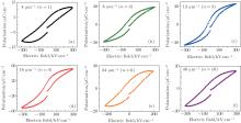
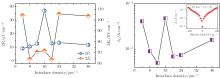
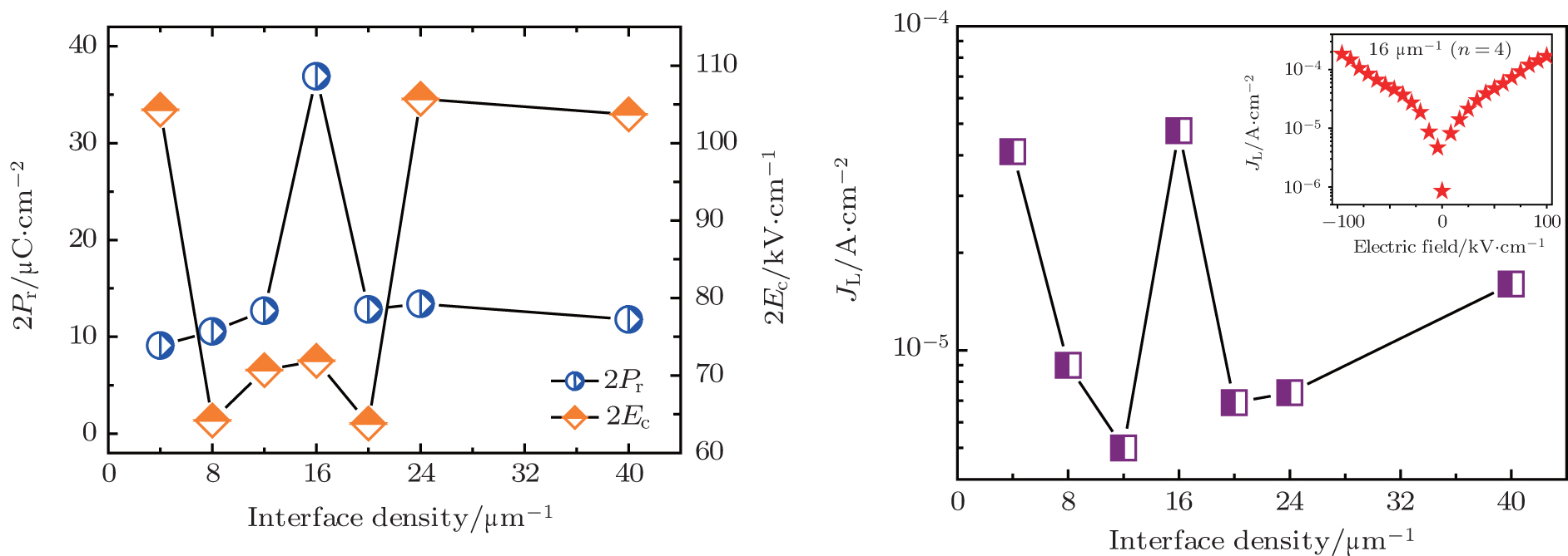
Figures 2(a)– 2(f) show the P– E loops of the (PSTT10/45)n multilayer thin films with different interface densities. Obviously, the (PSTT10/45)4 films with an interface density of 16 μ m− 1 exhibit larger remnant polarizations and better loop shapes than the other films. The remnant polarizations, coercive fields, and leakage current densities of the (PSTT10/45)n multilayer thin films each as a function of interface density are shown in Figs. 3(a) and 3(b), where the inset shows a typical leakage current of the film with n = 4. All of the electrical properties of the (PSTT10/45)n multilayer thin films are summarized in Table 1. Approximately, the 2Pr value increases with the increase of Ni/d, reaches a maximum (2Pr = 36.9 μ C/cm2) at Ni/d = 16 μ m− 1, and then decreases with the further increase of Ni/d. The corresponding shape of P– E loop also exhibits a tendency of saturation from Ni/d = 4 μ m− 1 to Ni/d = 16 μ m− 1, then becomes undersaturated with the further increase of Ni/d. Each of the films shows a low coercive field at low interface density (Ni/d = 8 μ m− 1– 20 μ m− 1), and exhibits a comparatively high coercive field as Ni/d exceeds 24 μ m− 1 (Ni/d = 24 μ m− 1, 40 μ m− 1), which is in the same level as those of the PSTT5 thin films.[22] The leakage current density of the film changes from several μ A/cm2 to several tens of μ A/cm2 with the change of interface density, and reaches a maximum at n = 4. As a result, the ferroelectric properties can be greatly influenced and optimized by configuring the interface density of (PSTT10/45)n multilayer thin film.
Fig. 2.P– E loops of the (PSTT10/45)n multilayer thin films each as a function of interface density, for n/d = 4 (a), 8 (b), 12 (c), 16 (d), 24 (e), and 40 μ m− 1 (f).
Fig. 3. (a) Remnant polarization and coercive field, and (b) leakage current density of the (PSTT10/45)n multilayer thin film as a function of interface density. Inset shows the typical leakage current of the film with n = 4.
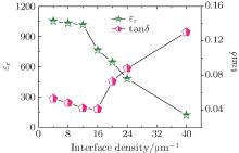
Figure 4 shows the relative dielectric constant (ε r) and the dielectric loss (tan δ ) of the (PSTT10/45)n multilayer thin film each as a function of interface density at 1 kHz. The curves can be divided into two sections: the ε r decreases slowly in the range of Ni/d = 4 μ m− 1– 12 μ m− 1, and then decreases rapidly from Ni/d = 16 μ m− 1 to Ni/d = 40 μ m− 1; correspondingly, the tan δ decreases slightly with the increase of Ni/d, reaches a minimum (0.041, Table 1) at Ni/d = 16 μ m− 1, and then increases rapidly with the further increase of Ni/d. For the dielectric constant and loss of the film, there exists a turning point from slow change to rapid change around Ni/d = 12 μ m− 1– 16 μ m− 1. In short, the dielectric properties can be modified by changing the interface density of the (PSTT10/45)n film.
Table 1. Electrical properties of the (PSTT10/45)n multilayer films.
4. Discussion
The interface density or periodicity in multilayer thin film has a key influence on the electrical properties of the film. With the increase of interface density or periodicity, the dielectric and ferroelectric properties of the multilayer thin films often increase and they reach optimum values (which may be maxima) at a critical point, and then decrease or degenerate with the further increase of interface density.[18– 20] In the PbZr0.2Ti0.8O3/PbZr0.4Ti0.6O3 multilayer thin films this critical point is Ni/d = 0.2 nm− 1; [18] in the [(Pb0.90La0.10)Ti0.975O3/PbTiO3]n ((PLT/PT)n) multilayer thin films this critical point is n = 2; [19] in the present (PSTT10/45)n multilayer thin films this critical point is Ni/d = 16 μ m− 1, although it has the largest leakage current at this point.
Feigl et al.[18] carefully investigated and summarized the influence of interface density on the properties of multilayer thin films, indicating that at lower interface densities with smooth interface, with the increase of the interface density, the decreased thickness of each layer makes the stress at the interface difficult to relax inside the layer, thereby increasing the overall stress of the films and thus enhancing the remnant polarization of the film. Moreover, the smoother interface increases the mobility of domain walls, which enhances the dielectric constant. The stress (lattice distortion) can be observed inside the (PLT/PT)n[19] and the present (PSTT10/45)n films (Fig. 1(b)). The above mechanism can appropriately explain the high remnant polarizations and dielectric constants of the (PLT/PT)n and the (PSTT10/45)n films at low interface densities, and it can also explain the reductions of coercive field of the two films. If the interface density is further increased, [18] a higher volume fraction of features such as interface defects and dislocations[28– 30] may result in the deteriorations of both Pr and ε r by local strains and space charge effects.[31– 34] Moreover, these distortions could reduce the mobility of the domains or pin them, [35] which would also contribute to a smaller dielectric constant. This mechanism is well consistent with the behaviors of the (PLT/PT)n and the (PSTT10/45)n films (decreased 2Pr and ε r) at high interface density (periodicity), and can also explain why the coercive fields of the two films become high at high interface density (periodicity). But there is also a confusion: the leakage current density relationship with interface density of the films seems pretty elusive. Why there is a peak at n = 4 is the object further study.
In summary, it is suggested that inside the multilayer thin film there is a possible competition between interface stress and interface defect. This possibly existent competition finally leads to a critical point: at the low interface density, if the interface stress is predominant, the electric properties of the films should be enhanced and reach an optimized value; if the interface defect is predominant with the further increase of interface density, the electric properties of the films should degenerate at high interface density; furthermore, small changes under the process condition of the films should lead to different competition results (for example, different critical points).
5. Conclusions
The (PSTT10/45)n multilayer thin films are deposited by RF magnetron sputtering technique and post-annealed by TSRTA method. The influence of the interface density Ni/d on the electrical properties of the films are investigated. The remnant polarizations of the films increase with the increase of Ni/d, reach a maxima abruptly at Ni/d = 16 μ m− 1, and then decrease with the further increase of Ni/d. The dielectric constants of the films are demonstrated to have high values at low interface densities, then drop off quickly as Ni/d exceeds 12 μ m− 1. Approximately, the coercive fields and the dielectric losses of the films exhibit low values at low interface density, then rise up rapidly as Ni/d values exceed 20 μ m− 1 and 16 μ m− 1, respectively. It is found that a critical point exists around Ni/d = 16 μ m− 1, and the optimal electric properties of films at Ni/d = 16 μ m− 1 are 2Pr = 36.9 μ C/cm2, 2Ec = 71.9 kV/cm, ε r = 765, tan δ = 0.041, correspondingly. The electrical behaviors of the films possibly result from the competition of interface stress with interface defect. The result shows that changing interface density of the multilayer thin film should be an effective way to modulate the electrical performance.
Acknowledgments
We wish to thank Dr. Zhang Chao-Liang of the State Key Laboratory of Oral Diseases in Sichuan University, and Mr. Jin Yong of the College of Materials Science and Engineering of Sichuan University, for help with SEM and XRD data, respectively.
SunY C, LiX D, ZhouY Y, LiH M, ZhuJ L, LiuH, PeiY, XiaoD Q and ZhuJ G200918th IEEE International Symposium on the Applications of FerroelectricsAugust 23–27, 2009Xi’an, Chinap. 210DOI:10.1109/ISAF.2009.5307580[Cited within:1]
24
LiX D, ChenQ, SunY C, ZhouY Y, ZhuJ L, XiaoD Q and ZhuJ G200918th IEEE International Symposium on the Applications of FerroelectricsAugust 23–27, 2009Xi’an, Chinap. 214DOI:10.1109/ISAF.2009.5307577[Cited within:3]
... 6] However, the Curie temperature (TC) of PST is between 0 and 25#cod#x00A0 ...
... [6,12] ...
1
2011
0.0
0.0
... To modify the features of the ferroelectrics, three methods are often used in preparation: doping,[7,8] substitution,[9] and solid solution ...
1
2014
0.0
0.0
... To modify the features of the ferroelectrics, three methods are often used in preparation: doping,[7,8] substitution,[9] and solid solution ...
1
2012
0.0
0.0
... To modify the features of the ferroelectrics, three methods are often used in preparation: doping,[7,8] substitution,[9] and solid solution ...
1
2013
0.0
0.0
... [10,11] Mixing PST with lead titanate (PbTiO3, PT), e ...
1
2012
0.0
0.0
... [10,11] Mixing PST with lead titanate (PbTiO3, PT), e ...
1
2000
0.0
0.0
... [6,12] ...
1
2007
0.0
0.0
... s electrical properties,[13#cod#x2013 ...
1
2009
0.0
0.0
1
2012
0.0
0.0
... 15] and an appropriate combination of the layers with different compositions can either improve the functional properties or create one or more novel properties ...
1
2010
0.0
0.0
... [16,17] Inside multilayer thin film, interfacial intensity[18] or periodicity[19,20] can greatly influence the electrical performance of the film ...
1
2007
0.0
0.0
... [16,17] Inside multilayer thin film, interfacial intensity[18] or periodicity[19,20] can greatly influence the electrical performance of the film ...
5
2009
0.0
0.0
... [16,17] Inside multilayer thin film, interfacial intensity[18] or periodicity[19,20] can greatly influence the electrical performance of the film ...
... [18#cod#x2013 ...
... [18] in the [(Pb0 ...
... [18] carefully investigated and summarized the influence of interface density on the properties of multilayer thin films, indicating that at lower interface densities with smooth interface, with the increase of the interface density, the decreased thickness of each layer makes the stress at the interface difficult to relax inside the layer, thereby increasing the overall stress of the films and thus enhancing the remnant polarization of the film ...
... If the interface density is further increased,[18] a higher volume fraction of features such as interface defects and dislocations[28#cod#x2013 ...
3
2009
0.0
0.0
... [16,17] Inside multilayer thin film, interfacial intensity[18] or periodicity[19,20] can greatly influence the electrical performance of the film ...
... [19] in the present (PSTT10/45)n multilayer thin films this critical point is Ni/d #cod#x003D ...
... The stress (lattice distortion) can be observed inside the (PLT/PT)n[19] and the present (PSTT10/45)n films (Fig ...
2
2007
0.0
0.0
... [16,17] Inside multilayer thin film, interfacial intensity[18] or periodicity[19,20] can greatly influence the electrical performance of the film ...
... 20] In the PbZr0 ...
2
2009
0.0
0.0
... In our previous work, various efforts have been made to improve the properties of PSTT single films, including the heat treatment of common rapid thermal annealing (RTA),[21] a novel two-step rapid thermal annealing (TSRTA) which can greatly reduce the duration of the film retained in high temperature,[22#cod#x2013 ...
... [21#cod#x2013 ...
4
2011
0.0
0.0
... In our previous work, various efforts have been made to improve the properties of PSTT single films, including the heat treatment of common rapid thermal annealing (RTA),[21] a novel two-step rapid thermal annealing (TSRTA) which can greatly reduce the duration of the film retained in high temperature,[22#cod#x2013 ...
... The films were then post-deposition annealed three times by the TSRTA method[22#cod#x2013 ...
... [22,26] Figure#cod#x00A0 ...
... [22] The leakage current density of the film changes from several #cod#x03BC ...
1
2009
0.0
0.0
3
2009
0.0
0.0
... 24] preparing Pb(Zr0 ...
... 24] with a peak temperature of 750#cod#x00A0 ...
... 24] The number of interfaces per micrometer Ni/d, with Ni being the number of interfaces (Ni #cod#x003D ...
1
2012
0.0
0.0
... 48)O3 (PZT52/48) as a seed layer,[25] and fabricating a composition differential multilayer thin film (PSTT10/45) ...
4
2014
0.0
0.0
... [26] Recently, epitaxial PST films with good ferroelectric properties were also grown on electroded and buffered Si#cod#x00A0 ...
... [26] Total thickness values of PSTT10 and PSTT45 films were both 250#cod#x00A0 ...
... [22,26] Figure#cod#x00A0 ...
... [26] ...
1
2013
0.0
0.0
... [27] ...
1
2005
0.0
0.0
... If the interface density is further increased,[18] a higher volume fraction of features such as interface defects and dislocations[28#cod#x2013 ...
1
2006
0.0
0.0
1
2009
0.0
0.0
... 30] may result in the deteriorations of both Pr and #cod#x03B5 ...
1
2010
0.0
0.0
... [31#cod#x2013 ...
1
2010
0.0
0.0
1
2007
0.0
0.0
1
2012
0.0
0.0
... 34] Moreover, these distortions could reduce the mobility of the domains or pin them,[35] which would also contribute to a smaller dielectric constant ...
1
2006
0.0
0.0
... 34] Moreover, these distortions could reduce the mobility of the domains or pin them,[35] which would also contribute to a smaller dielectric constant ...
The interface density dependence of the electrical properties of 0.9Pb(Sc0.5Ta0.5)O3–0.1PbTiO3/0.55Pb(Sc0.5Ta0.5)O3–0.45PbTiO3 multilayer thin films
[Li Xue-Donga),b), Liu Hongb), Wu Jia-Gangb), Liu Ganga), Xiao Ding-Quanb), Zhu Jian-Guo†b)]


 ]
]