


Lumped-equivalent circuit model for multi-stage cascaded magnetoelectric dual-tunable bandpass filter
[Zhang Qiu-Shi, Zhu Feng-Jie, Zhou Hao-Miao† ]
]
]
|
|


†Corresponding author. E-mail: zhouhm@cjlu.edu.cn
*Project supported by the National Natural Science Foundation of China (Grant Nos. 11172285 and 11472259) and the Natural Science Foundation of Zhejiang Province, China (Grant No. LR13A020002).
A lumped-equivalent circuit model of a novel magnetoelectric tunable bandpass filter, which is realized in the form of multi-stage cascading between a plurality of magnetoelectric laminates, is established in this paper for convenient analysis. The multi-stage cascaded filter is degraded to the coupling microstrip filter with only one magnetoelectric laminate and then compared with the existing experiment results. The comparison reveals that the insertion loss curves predicted by the degraded circuit model are in good agreement with the experiment results and the predicted results of the electromagnetic field simulation, thus the validity of the model is verified. The model is then degraded to the two-stage cascaded magnetoelectric filter with two magnetoelectric laminates. It is revealed that if the applied external bias magnetic or electric fields on the two magnetoelectric laminates are identical, then the passband of the filter will drift under the changed external field; that is to say, the filter has the characteristics of external magnetic field tunability and electric field tunability. If the applied external bias magnetic or electric fields on two magnetoelectric laminates are different, then the passband will disappear so that the switching characteristic is achieved. When the same magnetic fields are applied to the laminates, the passband bandwidth of the two-stage cascaded magnetoelectric filter with two magnetoelectric laminates becomes nearly doubled in comparison with the passband filter which contains only one magnetoelectric laminate. The bandpass effect is also improved obviously. This research will provide a theoretical basis for the design, preparation, and application of a new high performance magnetoelectric tunable microwave device.
Magnetoelectric (ME) laminated composite materials can connect the ferromagnetic phase and the ferroelectric phase through using the stress– strain as the medium, which makes the energy convert freely between the magnetic field and electric field through the direct and converse ME coupling effect. Therefore, the ME laminated composite material has attracted more attention in academic and industry communities because of the prospect of its broad application in miniaturized, multi-functional, integrated, and smart devices.[1– 4] Many studies have been done on the positive ME coupling effect, which allows the magnetic signal to induce the output of an electric signal, especially on the nonlinear ME coupling effect with consideration of the variable temperature environment and the different stress environment.[5– 9] The theoretical studies have promoted the applications of new devices using ME laminated composite materials, such as a high precision sensor for a weak magnetic field, [10] an energy harvester, [11– 13] a current-to-voltage converter, [14] a voltage transformer, [15] etc. Studies of the converse ME effect in ME laminated composite materials mainly focus on the new tunable device design and the involved microwave ME mechanism in ME dual-tunable microwave device, which consists of the ME laminated composite materials and the microwave device.[16] Compared with traditional magnetically tunable or electrically tunable microwave devices, this type of novel ME dual-tunable microwave device has special excellent performance, such as low power consumption, low noise, high quality, “ coarse magnetic tunability” , and “ precise electrical tunability” .[2, 17, 18] Therefore, the ME material has broad potential applications in the field of high technology, such as electronic warfare systems, future communication systems, and an active phased array radar in a national defense platform.[1, 19]
As early as in 2001, Bichurin et al.[20] established a phenomenological theory of the microwave ME coupling effect in ME composite materials. In 2002, they established a theory about magnetic and ME susceptibilities under microwave frequencies.[21] In their work, they gave the expression of the equivalent bias field under the electric field exerted on the piezoelectric phase. For the first time, they pointed out in theory that the external electric and magnetic field can tune the ferromagnetic resonance (FMR) frequency of a ME laminated composite material which can be used in the design of tunable microwave devices. Many experimental studies have followed, which have explored the material properties and the ME coupling properties of different ME composite materials at microwave frequencies.[22– 31] These studies strongly promoted the applications of ME composite materials in tunable microwave devices. For example, Srinivasan et al.[32] proposed that placing the YIG/PMN-PT on a microstrip filter can realize the electric field-tunable microwave filters. Tatarenko et al. designed an ME dual tunable bandpass filter through combining the ME laminate material with two straight microstrip lines.[33] It was also found that Zn2Y/PMN-PT can improve the ME conversion coefficient through comparing the properties of the resonator with those of the laminates Zn2Y/PZT and Zn2Y/PMN-PT, respectively.[34] Afterwards, they used the M-type hexagonal ferrite (BaM) to design a phase shifter whose phase can be tuned precisely.[35] Chen et al. found a big drift of the FMR frequency when the permeability of the Z-type Ba ferrite doping Co element changed, thereby providing the basis for applications that use the Z-type ferrite in tunable microwave devices.[36] Yang et al. designed a symmetrical T-type microstrip transducer through changing the microstrip line structure[37] and using the ferrite sandwich structure on the microstrip filter to enhance the frequency shift.[38] Then, Yang et al. used partially magnetized ferrites, which have a wide frequency-tunable range at low magnetic fields, to design a low loss, miniaturized tunable bandpass filter[39, 40] and a tunable low power phase shifter.[41] Subsequently, they proposed an electric tunable phase shifter containing one ferromagnetic layer and two piezoelectric layers, which can effectively improve the tunable range of the frequency drift[42] induced by the electric field. Based on magnetostatic surface wave (MSSW) theory, Wu et al.[43] changed the offset angle of the ferrite placed on the invert L-shaped microstrip lines and realized a nonreciprocal tunable bandpass filter with high isolation. Although there are large numbers of studies of ME-tunable microwave devices, there are many disadvantages in ME devices, such as the narrow bandwidth and the bad bandpass effect.
Usually, in the process of designing a functional material microwave device which contains a magnetic medium or an electric medium, the electromagnetic (EM) field simulation is used to design the device in advance to reduce the design difficulty and reduce the complexity of the work. For the EM field simulation of the functional material microwave device, the calculation is very heavy and much time will be taken. If the lumped-equivalent circuit model for this kind of device can be established to capture the important characteristics (such as the passband frequency and bandwidth) in advance, then it can greatly shorten the design time and improve design efficiency. For example, Marcelli et al.[44] established a lumped-equivalent circuit model for a magnetostatic wave (MSW) straight edge resonator. Tsai et al.[45] established a lumped-equivalent circuit model for a magnetic tunable bandstop filter by using YIG/GGG-GaAs laminate structure. However, for the magnetic field and electric field dual tunable microwave device composed of ME-laminated composite materials, only Zhou et al.[46– 49] carried out research of a lumped-equivalent circuit. For instance, they established lumped-equivalent circuit models for the ME-tunable single microstrip resonator[46] and coupling microstrip filter, [47] respectively. Later, Srinivasan et al.[50] pointed out that using multi-block ME laminates to design tunable microwave devices can effectively improve the device bandwidth and overcome shortcomings of the microwave device with one block ME laminate, such as the worse passband effect, narrow bandwidth, and inability to realize the dual-passband and multi-passband. For this purpose, Zhou et al.[48, 49] further set up an effective lumped-equivalent circuit model for the ME dual-tunable single microstrip microwave device[48] and coupling microstrip microwave device, [49] which contains multi-block ME-laminates. But for the switch-controllable multi-stage cascaded ME-tunable bandpass filter with multi-block ME-laminates, which may have a better bandwidth broadening effect, few relevant research reports are published on the device design or on the lumped-equivalent circuit.
In view of the disadvantages (such as the narrow bandwidth and bad passband effect) in current ME-tunable microwave devices, a multi-stage cascaded ME-tunable bandpass filter with a plurality of ME laminates is proposed and the lumped-equivalent circuit model for the filter is established in this paper. The validity of the lumped circuit model is verified through degrading the lumped-equivalent circuit model and comparing it with the already existing experiment measurement results for the filter with one block of ME laminate. On this basis, the ME-dual tunable and switch-controllable characteristics of the multi-stage cascaded ME filter model are further analyzed. Then, compared with the coupling microstrip filter with only one ME laminate, the multi-stage cascaded filter with multi-block ME laminates has the passband bandwidth broadened nearly twice under the same magnetic field.
A multi-stage cascaded ME-tunable bandpass filter model with a number of ME laminates is shown in Fig. 1. The filter contains n-block ME laminates (n ≥ 2) and the dielectric substrate, input, and output microstrip line and (m = n − 1) short microstrip lines, which are placed alternately with n-block ME laminates. The width and thickness of the i-th short microstrip line are wi and ti, respectively. The width and thickness of the input microstrip are win and tin, respectively. Correspondingly, the width and thickness of the output microstrip are wout and tout. The n-block ME laminates have the same size, consisting of n piezoelectric layers and n ferrite layers which are bonded by the epoxy. The size of the ferrite is lf × wf × tf, and the saturation magnetization is Ms. The FMR linewidth is Δ H. The passband frequency of the filter is tunable in a big range by applying the static fields H1, H2, … , Hn to an arbitrary direction through permanent magnets or electric coils. The size of the piezoelectric layer is lp × wp × dp, and two metal films are plated on the upper and lower surfaces of the piezoelectric layer as electrodes. Precise regulation can be realized in a small range when the external electric fields E1, E2, … , En are applied to the electrodes.
 | Fig. 1. Model of the multi-stage cascaded filter with a number of ME laminates. |
The electromagnetic wave signal is applied to the input microstrip line from the Pin for transmission in Fig. 1. According to the theory of mutual coupling characteristics between the transport current and MSW, [51] when the same magnetic or electric fields are applied to n-block ME laminates, the electromagnetic wave signal in the input microstrip is transmitted to the first ME laminate. The electromagnetic wave signal near the FMR frequency is then transmitted to the first short microstrip through the coupling effect between the first ME laminate and the first short microstrip. Afterwards, the signal near the same FMR frequency is transmitted to the second short microstrip through the coupling effect between the first short microstrip and the second ME laminate. The rest can be deduced by analogy. Finally, the electromagnetic wave signal near the FMR frequency on the ME laminate is transmitted to the output microstrip and outputted as Pout to achieve the band-pass effect. If the applied magnetic or electric fields in arbitrary two ME laminates between the n-block ME laminates are different, then the passband of the filter will be cut off. Taking the cascaded filter with two ME laminates as an example, when the applied magnetic and electric field are H1 and E1 and assuming the FMR frequency is f1, the electromagnetic wave signal near f1 will be transmitted to the short microstrip 1 through the coupling effect. If the applied magnetic field H2 or electric field E2 to the second ME laminate is different from that applied to the first ME laminate, then the FMR frequency f2 in the second ME laminate will be different from f1. In this case, the signal will be transmitted to the output microstrip only near the f2 through the second ME laminate. So, when the difference between the f1 and f2 reaches a certain level, the electromagnetic wave signal in the short microstrip, which is transmitted from the first ME laminate through the coupling effect, will not be transmitted by the second ME laminate, the passband of the filter will disappear, and the filter becomes an isolator. In summary, the above device can be controlled whether the signal can be transmitted effectively or not through applying the magnetic field or electric field to different ME laminates. That is to say, when the applied magnetic fields and electric fields are the same, respectively, between the n-block ME laminates, then the filter will be a bandpass filter whose passband is tunable. When the fields are differently applied to different ME laminates, the filter will be cut off and this will achieve the effect of a switch. This provides a new idea for researchers to change or improve the properties of devices in designing ME microwave devices.
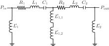
As for the ME dual-tunable band-pass filter in Fig. 1, its lumped-equivalent circuit model is established according to its electromagnetic coupling transmission characteristics. When the electromagnetic wave signal is transmitted to the first ME laminate from the input microstrip, the coupling inductance 


 | Fig. 2. Lumped-equivalent circuit model of the multi-stage cascaded ME-tunable bandpass filter. |
Then, for the lumped-equivalent circuit model in Fig. 2, the concrete expressions of the electrical components are derived in the following description. Taking the effects of the magnetic anisotropy field Han[52] and demagnetizing field Hdem[53] into consideration, when the static magnetic field Hi (Hix, Hiy, Hiz) in an arbitrary direction is applied to the i-th ME laminate, the expressions of FMR frequency fi of ferrite in the directions of the x, y, z axes can be obtained as follows:[47]

where Nx, Ny, and Nz are the demagnetizing factors along the x, y, and z axes; Mx, My, and Mz are the magnetic components along the x, y, z axes, respectively; and, γ is the gyromagnetic ratio.
Next, the regulation of the FMR frequency in ferrite layer, when an electric field is applied to the piezoelectric layer, is considered. The piezoelectric layer deforms when the external electric field Ei is exerted on the i-th ME laminate. According to the binding effect in the ME laminate, the deformation will be transferred to the ferrite layer so that some parameters such as the permeability of ferrite will be changed. Consequently, the FMR frequency will be changed too. The change of the frequency has a similar effect to the change of frequency through the changed external magnetic field. So, it can be described by an equivalent magnetic field δ HE(i) = AEi induced by the electric field. The expression of the ME conversion factor A is given as[54]

The left superscript “ p” of each parameter represents the piezoelectric layer, pS11 and pS12 are compliance coefficients of the piezoelectric layer, pd13 is the piezoelectric coefficient of the piezoelectric layer. λ s is the magnetostrictive coefficient of the ferrite layer. The ck (ck ≥ 1) is the coupling coefficient which is used to describe the strain transmission on interface between piezoelectric layer and ferrite layer. This means that the strain induced by the electric field in the piezoelectric layer is equal to the transmitted strain in the ferrite layer, multiplied with the coupling coefficient ck. Obviously, when ck = 1, the interface is in an ideal condition and the strain in the piezoelectric layer can be transmitted to the ferrite layer completely. In this case, the ME conversion factor A reaches its maximum. When ck > 1, there will be more interface defects, an easier slip on interface, and a smaller strain will be transmitted to the ferrite layer. In this case, the ME conversion factor A will become smaller.
By considering the equivalent magnetic field induced by the external electric field, the effective magnetic field 

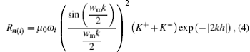
According to the interaction theory of the MSW and current, [51] the radiation resistance per unit length Rn(i) is introduced to represent the interaction theory. The radiation resistance Ri is then obtained by the effective length of the ME laminate. The radiation inductance Li and the radiation capacitance Ci can also be obtained by using the definition of the quality factor in the series resonant circuit. For the arbitrary i-th ME laminate, the radiation resistance per unit length Rn(i)[51] is
where ω i = 2π fi is the FMR resonance angular frequency, μ 0 is the permeability of vacuum, h is the distance from the current in microstrip to the ferrite layer, 
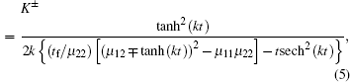
where t is the distance from the ferrite layer to the ground; and, μ 11, μ 12, and μ 22 are the components of relative permeability. In a case where the magnetostatic volume wave is induced in the ferrite layer, 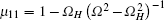


Considering the transmission characteristics of the narrow-band filter, the radiation resistance Ri in the arbitrary i-th ME laminate can be obtained by the radiation resistance per unit length:

In a normal situation, when Ri is obtained, the unload quality factor Q0 = fi/(γ × Δ H) can be obtained by using the resonance linewidth Δ H, and the Li or Ci can be obtained by using the definition of the quality factor in a series resonant circuit. However, according to the results obtained by Marcelli et al., [44] when the ferrite layer is placed in the middle of the coupling microstrip, the equivalent radiation inductance needs to take account of the coupling effect between the microstrip and the ME laminate. Consequently, the equivalent radiation inductance and the radiation capacitance can be modified as follows:


where the coupling factors 


where D is the distance between the ME laminate and the short microstrip, 


where Z0 is the characteristic impedance, ta is the thickness of the dielectric substrate, 
Similarly, the other expressions of the coupling inductance between the ME laminate and the microstrip can be obtained by the coupling factors from Eqs. (9) and (10):


If all of the short microstrips have the same dimension, namely the two-port network is a reciprocal network, when the filter fulfills the electric matching, then the external quality factor 
In summary, for the lumped-equivalent circuit model in Fig. 2, combining component parameters from Eqs. (6)– (8) with those from Eqs. (13)– (16), the lumped-equivalent circuit model of the multi-stage cascaded ME-tunable bandpass filter is established in this paper.
As for the lumped-equivalent circuit model of the multi-stage cascaded ME-tunable bandpass filter mentioned above, in order to verify the validity of the model, the experimental result is adopted in Ref. [33] which is a ME-tunable bandpass filter that contains one block of ME laminate between two coupling microstrips. Since the lumped-equivalent circuit model is used for the multi-stage cascaded ME-tunable bandpass filter containingn-block ME laminates, the model is degraded to the case that n is set to be 1 in order to meet the experimental conditions in Ref. [33]. The relevant parameters in the lumped-equivalent circuit model are consistent with Ref. [33] in experimental conditions. For example, the ferrite layer YIG film is chosen, the size is 5.5 mm × 1.5 mm × 0.11 mm, the saturation magnetization is 4π Ms = 1750 Gs (1 Gs = 10− 4 T), and the YIG film is grown on a GGG substrate by the liquid phase method. The piezoelectric layer PZT material is chosen with a size of 4 mm × 1 mm × 0.5 mm. Two metal films are plated on the upper and lower surfaces of the piezoelectric layer as electrodes to which the external electric field E is applied. The YIG film and PZT layer are bonded by the epoxy. The dimensions of the input and output microstrips are 18 mm × 1 mm × 18 mm and the microstrips meet the requirement for the 50-Ω matching with the substrate (ε = 10).
When the bias magnetic field is applied along the x direction, and the value H = 1.7 kOe (1 Oe = 79.5775 A· m− 1) keeps unchanged, the ME conversion factor A = 13 Oe· cm/kV can be obtained by the geometry dimensions and the material parameters of the ME laminate. Each electrical component value can be obtained from Eqs. (6)– (8) and (13)– (16). Then, when the values of external electric field E are 0 kV/cm, 1 kV/cm, and 2 kV/cm, the insertion loss is calculated by using the lumped-equivalent circuit model. To conveniently validate the effectiveness of the equivalent circuit, commercial electromagnetic field simulation (EM field simulation) software is used to simulate the physics model mentioned in Ref. [33] for the full-wave analysis. A comparison of insertion loss among the experimental result in Ref. [33], the predicted result by the circuit model, and the EM simulation result are shown in Fig. 3. As shown in Fig. 3, the predicted result of the insertion loss in lumped-equivalent circuit model is in good agreement with the experimental measurement, and it can effectively describe the peak phenomenon occurring in the insertion loss curves due to the FMR. Meanwhile, the predicted FMR frequency is also in good agreement with the experimental result. From the comparison of the above results, it can be seen that the lumped-equivalent circuit model is valid.
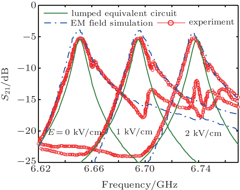 | Fig. 3. Insertion loss curves for the ME-tunable coupled microstrip filter with one block ME laminate. |
To further validate the effectiveness of the established lumped-equivalent circuit model (Fig. 2), a filter that is composed of two ME laminates is selected for analysis (n = 2 in Fig. 2). The two-stage cascaded ME dual-tunable filter contains two ME laminates and three microstrips (one short microstrip, input, and output microstrips). For simplicity, the parameter settings in two blocks are in agreement with those in the above-mentioned filter which contains only one block ME laminate. The filter is placed between the two coils, which produces an external magnetic bias field Hi along the x axis.
According to the ME dual-tunable bandpass filter with two ME laminates (n = 2) and based on the above derivation process, the lumped-equivalent circuit shown in Fig. 2 can be simplified into the lumped-equivalent circuit shown in Fig. 4, where 


 | Fig. 4. Lumped-equivalent circuit model of the cascaded tunable bandpass filter containing two ME laminates. |
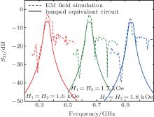
According to the geometry and material parameters of the ME laminate material, microstrips and substrate for the two-cascaded tunable bandpass filter, based on the Eqs. (6)– (8) and (13)– (16), each component in the equivalent circuit shown in Fig. 4 can be determined in turn. When the external electric fields are ignored in the two blocks and the applied bias magnetic fields are the same, i.e., E1 = E2 = 0 kV/cm and H1 = H2 = H, the curve of insertion loss is obtained in Fig. 5 when the bias magnetic field varies from 1.6 kOe to 1.8 kOe. As shown in Fig. 5, when the bias magnetic fields applied to both the ME laminates are identical, the insertion loss curves drift when the bias magnetic field changes, so the pass-band of the filter can be changed by an external magnetic field. Meanwhile, it can also be seen from Fig. 5 that the predicted results of the lumped-equivalent circuit are in good agreement with the EM field simulation and can effectively capture the characteristics of passband frequency, bandwidth, and the passband frequency drift under the external bias magnetic field H = H1 = H2 = 1.7 kOe. Secondly, when the external bias magnetic field and the applied electric fields are taken to be 0 kV/cm, 1 kV/cm, and 2 kV/cm, the predicted curves of the insertion loss by the lumped-equivalent circuit and the EM field simulation are shown in Fig. 6. As can be seen from Fig. 6, both the insertion loss curves predicted by the two methods are basically consistent, no matter whether they are in the passband frequency or the passband bandwidth. The passband frequency shifts towards the right as the electric increases, that is to say, the electric field can tune the filter passband. The validity of the lumped-equivalent circuit model can be further verified by the results from Figs. 5 and 6.
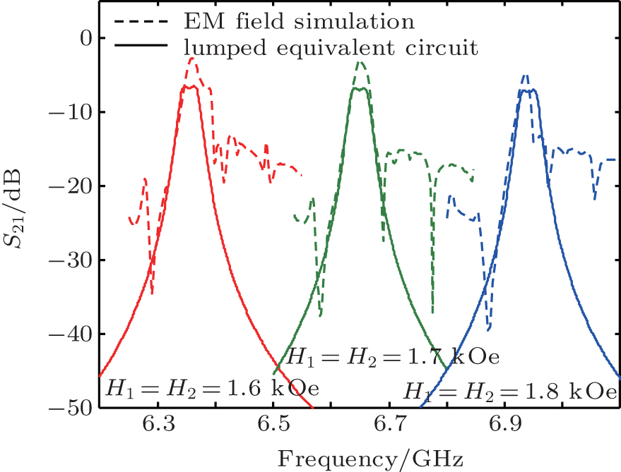 | Fig. 5. Curves of insertion loss versus frequency under different static magnetic fields. |
 | Fig. 6. Curves of insertion loss versus frequency under different static electric fields. |
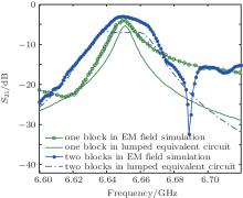
Next, the performance characteristics of the cascaded filter that uses multi-block ME laminates are discussed. For the filter that contains one and two ME laminates mentioned above, both the external magnetic field and the electric field applied to the one or two ME laminates are taken as 1700 Oe and 0 kV/cm, respectively. The insertion loss curves of the bandpass filters which contain one and two ME laminates, respectively, are shown in Fig. 7. From Fig. 7 it can be seen clearly that no matter whether one block ME laminate or two-blocks ME laminates are placed on the cascaded filter, the predicted insertion loss curves by the lumped-equivalent circuit and EM field simulation results are basically consistent. Moreover, the predicted result obtained by using two ME laminates is more consistent with the result obtained by using one block ME laminate for the lumped-equivalent circuit and the EM field simulation. The − 10-dB bandwidth for the two-stage cascaded filter is about 40 MHz, which is obtained from both the lumped-equivalent circuit and the EM field simulation. But for the one block filter, the − 10-dB bandwidth is only about 20 MHz. That is to say, compared with the ME-tunable bandpass filter that contains only one ME laminate, the − 10-dB bandwidth is broadened nearly twice as large as that for the filter using two ME laminates.
 | Fig. 7. Curves of Insertion loss versus frequency of the bandpass filter containing one and two ME laminates respectively. |
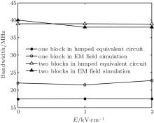
If the external electric fields applied to the ME laminates are different, then the variations of − 10-dB bandwidth with external electric field, predicted by the circuit model and EM field simulation, respectively, for one and two ME laminates are shown in Fig. 8. As can be seen in Fig. 8 clearly, when the result is predicted by the lumped-equivalent circuit model, the variations of − 10-dB bandwidth keeps unchanged under different electric fields for the filters containing one and two ME laminates. While for the EM field simulation, the slight variations of − 10-dB bandwidth under different electric fields occur. But whether the result is predicted by lumped-equivalent circuit or the result is obtained by the EM field simulation, it is clearly shown that the − 10-dB bandwidth for the two-stage cascaded filter is broadened to nearly twice as large as that for the filter with only one ME laminate.
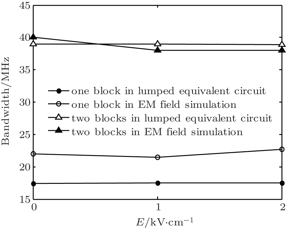 | Fig. 8. Plots of − 10-dB bandwidth versus electric field, predicted respectively by the circuit model and EM field simulation under different electric fields. |
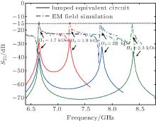
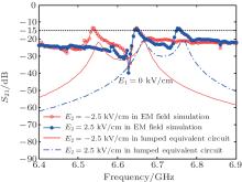
For the multi-stage cascaded filter, if the magnetic fields or electric fields applied to arbitrary two ME laminates are different, then the switching performance can be realized in the filter: the filter can be controlled to open or stop. Taking the two-stage cascaded filter discussed above as an example, keep the magnetic field on the first ME laminate unchanged (H1 = 1.7 kOe), set the magnetic field on the second ME laminate to be 1.9 kOe, 2.1 kOe, and 2.3 kOe separately and the bias magnetic field for the y direction. The predicted insertion loss curves of the lumped-equivalent circuit and the EM field simulation are shown in Fig. 9. In Fig. 9 the predicted result from the circuit model or the EM field simulation results can be clearly seen. The maximum insertion loss is nearly − 15 dB, that is to say, if different magnetic fields are applied to different ME laminates, the bandpass filter works in the stopped state and becomes a facto isolator. Similarly, keep the magnetic field on two ME laminates unchanged (H1 = H2 = 1.7 kOe), a similar effect of the filter converted to the isolator can also be achieved when applying different electric fields to different ME laminates. Keep the applied electric field on the first ME laminate unchanged (E1 = 0 kV/cm) and set the electric field on the second ME laminate to be E2 = − 2.5 kV/cm, and E2 = 2.5 kV/cm separately. Both the results predicted by the lumped-equivalent circuit and the EM field simulation results are shown in Fig. 10. From Fig. 10, it can be seen clearly whether the result is predicted by lumped-equivalent circuit or if the result is obtained by the EM field simulation, the maximum insertion loss is nearly − 15 dB. That is to say, if applying different electric fields to different ME laminates, the bandpass filter also works in the stopped state and becomes a facto isolator. As shown in Figs. 9 and 10, as long as the applied magnetic or electric fields in different ME laminates are not consistent through regulation, the signal will be cut off effectively, thereby converting the bandpass filter into an isolator.
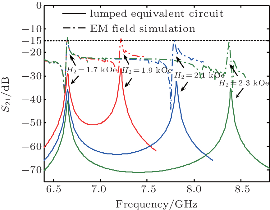 | Fig. 9. Curves of insertion loss versus frequency under different magnetic fields. |
 | Fig. 10. Curves of insertion loss versus frequency under different electric fields. |
It can be seen from the above analysis that by comparison with the EM field simulation, the predicted operating frequency by the lumped-equivalent circuit is often in good agreement with the experimental result and the EM field simulated result. But for the passband bandwidth, the EM field simulated result is closer to the experimental result than that from the lumped-equivalent circuit. So the EM field simulation result is more reliable than the result from the lumped-equivalent circuit. For the ME microwave device with simple microstrip structure, such as the straight microstrip structure, the coupling microstrip structure and the symmetric-T microstrip structure, it is easy to build a lumped-equivalent circuit model that can be used to analyze the device performance and the predicted results are also pretty effective. However, for a device with a complicated microstrip structure in practical engineering applications, it is very difficult to establish the equivalent circuit when the ME laminate is introduced. Therefore, when engineers design a complicated high-performance ME-tunable microwave device, the complicated microstrip structure can be analyzed by the EM field simulation, and the ME-tunable units can be analyzed by several typical lumped-equivalent circuits of a ME microwave device. In this case, it can not only utilize the advantage of fast and precise analysis for the EM field simulation when simulating the complicated microstrip structure but also avoid the shortage of time-consuming, heavy calculations, and big offsets when the ME functional material is contained.
In this paper, the lumped-equivalent circuit model is established for a multi-stage cascaded ME-tunable bandpass filter with a plurality of ME laminates, which can effectively broaden the bandwidth and improve the passband characteristics. The model’ s validity is verified through comparing the experimental result and EM field simulation result. After that, the model is degraded to the two-stage cascaded filter with two ME laminates. If the bias magnetic or electric fields applied to the two ME laminates are consistent, then the ME filter will produce a passband, whose bandwidth broadens nearly twice as large as that of the filter which contains only one ME laminate. If the magnetic or electric fields applied to the two ME laminates change at the same time, then the passband of the filter will be shifted and the lumped-equivalent circuit prediction result is basically consistent with EM field simulation result. Consequently, the effectiveness of the tunable characteristic predicted by the lumped-equivalent circuit model is further verified. If the external bias magnetic or electric fields applied to the two ME laminates are different for the two-stage cascaded filter, then the results obtained by the lumped-equivalent circuit and the EM field simulation results both reveal that the insertion loss of the filter decreases to − 15 dB; that is to say, the passband disappears so that the switching characteristic is achieved. This research and these conclusions will be helpful for designing, fabricating, and using the new high-performance ME-tunable microwave devices.
| 1 |
|
| 2 |
|
| 3 |
|
| 4 |
|
| 5 |
|
| 6 |
|
| 7 |
|
| 8 |
|
| 9 |
|
| 10 |
|
| 11 |
|
| 12 |
|
| 13 |
|
| 14 |
|
| 15 |
|
| 16 |
|
| 17 |
|
| 18 |
|
| 19 |
|
| 20 |
|
| 21 |
|
| 22 |
|
| 23 |
|
| 24 |
|
| 25 |
|
| 26 |
|
| 27 |
|
| 28 |
|
| 29 |
|
| 30 |
|
| 31 |
|
| 32 |
|
| 33 |
|
| 34 |
|
| 35 |
|
| 36 |
|
| 37 |
|
| 38 |
|
| 39 |
|
| 40 |
|
| 41 |
|
| 42 |
|
| 43 |
|
| 44 |
|
| 45 |
|
| 46 |
|
| 47 |
|
| 48 |
|
| 49 |
|
| 50 |
|
| 51 |
|
| 52 |
|
| 53 |
|
| 54 |
|
| 55 |
|