
Lateral resistance reduction induced by light-controlled leak current in silicon-based Schottky junction
[Wang Shuan-Hu†a)  , Zhang Xu
a) , Zou Lv-Kuana) , Zhao Jinga) , Wang Wen-Xina), b) , Sun Ji-Ronga) ]
, Zhang Xu|
|


†Corresponding author. E-mail: wshtzg@126.com
*Project supported by the National Basic Research Program of China (Grant No. 2011CB921801) and the National Natural Science Foundation of China (Grant No. 111374348).
Lateral resistance of silicon-based p-type and n-type Schottky junctions is investigated. After one electrode on a metallic film is irradiated, the differential lateral resistance of the system is dependent on the direction of the bias current: it keeps constant in one direction and decreases in the opposite direction. By systematically investigating the electrical potential changes in silicon and the junction, we propose a new mechanism based on light-controlled leak current. Our work provides an insight into the nature of this phenomenon and will facilitate the advanced design of switchable devices.
Schottky junctions have been studied extensively for more than half a century, [1] and numerous applications based on them have been realized or proposed.[2– 5] The photovoltaic effect (PVE), a main characteristic of a Schottky junction, has gained much attention due to its promise for many applications, such as high-efficiency solar cells.[3, 4, 6– 8] The illumination of light can excite the electrons to the conductance band, leaving holes in the valence band. The electron-hole pairs in a Schottky junction can then be separated by a built-in field. The lateral PVE (LPVE) refers to the potential difference on one side of the junction caused by the concentration gradient of photogenerated non-equilibrium carriers.[9, 10] Recently, our team has realized the magnetic tuning of LPVE in a silicon-based Schottky junction.[11] A new phenomenon observed in Schottky junction is the bipolar resistance effect (BRE), [12] which has drawn much attention due to its potential application in non-volatile memory.[13, 14] Laser-induced carriers which diffuse at the same or opposite direction can be applied to the field-driven drift electrons to generate bipolar resistance effect, which is attributed to the difference in scattering probability between equilibrium and non-equilibrium carriers.[12] This theory seems suitable for many Schottky junction systems. However, this effect has been rarely reported[15] and the method of resistance measurement is not clearly given. Therefore, regarding the lack of compelling evidence in this aspect, we think it is of great interest to explore the nature of light-induced bipolar resistance effect. Here, we perform some experiments in both p-type (Ta/p-Si) and n-type (Pt/n-Si) Schottky junctions. The results show that resistance keeps constant in one direction of external bias but decreases in the opposite direction. A new mechanism based on light-controlled leak current in silicon is proposed to explain this phenomenon.
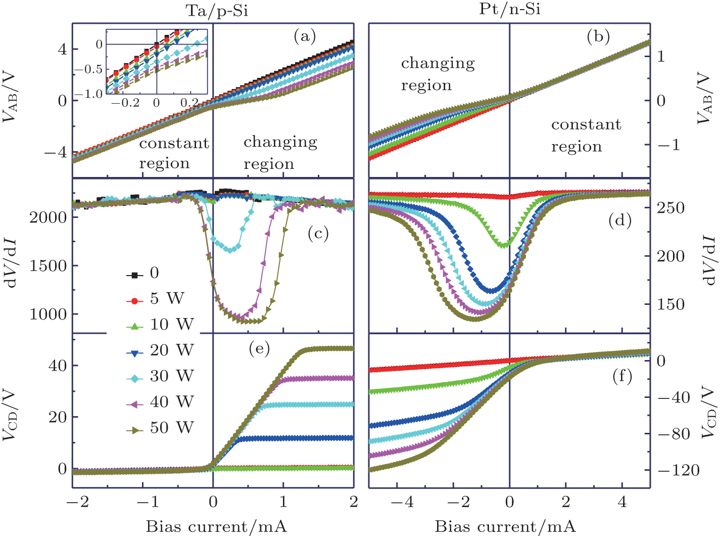
Samples were prepared by depositing, via magnetron sputtering, in an Ar atmosphere of 0.5 Pa, a 5-nm-thick Ta film or a 5-nm-thick Pt film through a 2 mm× 15 mm mask on p-type or n-type (001)-Si substrate (20 mm× 8 mm× 0.5 mm), respectively. The doping concentrations of both n-type and p-type silicon were both about 1015 cm− 3. The film thickness was calibrated by low-angle x-ray reflectivity. Silver paint and aluminum ultrasonic bonding were used for electric connection with the film and the Si substrate, respectively (Fig. 1(a)). To obtain an Ohmic Si– Al contact, a voltage pulse of 100 V was applied to break the possible interfacial barrier. The I– V characteristics of Si– Al after breakdown are shown in Fig. 1(c), and they show linear relation. A continuous laser beam (wavelength 635 nm) with tunable power was used to generate electron– hole pairs. The entire sample except the illuminated region was covered by an opaque soft mask during the measurements and all of the experiments were conducted under ambient conditions.
 | Fig. 1. (a) Sketch of the experimental setup, where two electrodes A and B on the film are used for injection and two probes C and D on the silicon substrate are used to detect the electric potential variation; (b) the band structure of p-type and n-type Schottky junction; (c) I– V curve of Al/Si contact. |
Figure 1(b) shows the band structure and distribution of photogenerated carriers in p-type and n-type Schottky junction. When a laser with energy higher than the bandgap in silicon is incident on the junction, electrons in the valence band will be excited to the conduction band, leaving holes in the valence band. In a Ta/p-Si system, photogenerated electrons will transfer to the Ta side according to the lowest energy principle, while the photogenerated holes prefer to stay on the p-Si side, as shown in left panel of Fig. 1(b). The holes and electrons will then diffuse from the illuminated spot. In contrast, in a Pt/n-Si system the photogenerated electrons stay on n-Si side and the holes tend to transfer to Pt side as shown in the right panel of Fig. 1(b).
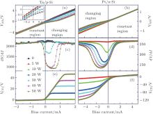
Figures 2(a) and 2(b) show the original current– voltage (I– V) characteristic curves varying with bias current under illumination, which is fixed at electrode A. All of the curves overlap in one direction, as shown in the left part of Fig. 2(a) and the right part of Fig. 2(b), which are both marked as the constant regions. In these regions, the film resistance is kept constant, regardless of how the illumination intensity varies. However, in the opposite direction, the curves become nonlinear as shown in the right part of Fig. 2(a) and the left part of Fig. 2(b), which are both marked as changing regions. In these regions, as the bias current increases from 0, the film voltage increases but deviates from the original tendency, and the degree of deviation is improved as the laser intensity increases. Since the existence of lateral photovoltage in the film (inset of Fig. 2(a)) leads to the deviation of the I– V curve from the original curve, it is irrational to use V and I measured by a voltmeter and an amperemeter to reflect the film resistance. Here, we use the differential resistance dV/dI instead. Figures 2(c) and 2(d) show the results of dV/dI calculated based on Figs. 2(a) and 2(b). A closer look at the curves finds that in the changing regions, dV/dI first rapidly decreases with a minimum at some place and then returns to the initial level, which is similar to the changes of resistance in the constant regions. The zone of minimum value is broadened and the amplitude decreases with the increase of laser power. Further calculation shows that the differential resistivity in the constant region is very similar to the result measured in the film which is attached on silicon with a 500-nm thermal oxide layer (27.2× 10− 7 Ω · m for Ta and 3.4× 0− 7 Ω · m for Pt). Hence, it can be concluded that under the laser illumination, the in-plane differential resistance of a metallic film is dependent on the direction of bias current, which is similar to previously reported result.[12] However, the phenomenon predicted by the theory that the resistance will be reversed after the reverse of bias [12] disagrees significantly with our results. In other words, the resistance reduction in our experiments is unidirectional.
 | Fig. 2. (a) and (b) I– V characteristic curves of the metallic film on Ta/p-Si and Pt/n-Si under varying illumination powers; (c) and (d) differential resistance calculated based on the data of panels (a) and (b); (e) and (f) I– V characteristic curves of the silicon substrate of Ta/p-Si and Pt/n-Si. |
Our first assumption to explain this phenomenon is to study the corresponding electrical potential change in silicon. As shown in Figs. 2(e) and 2(f), the evolution of voltage in silicon remarkably corresponds to the differential resistance in the film. In the constant region, the silicon voltage remains nearly unchanged and approximates to zero with the variation of the bias current. In the changing region, the silicon voltage obviously increases, and the increasing rate is improved with the enhancement of illumination power, indicating that a portion of the current flows through the substrate. When the V(Si) is saturated, the differential resistance returns to the original level. Hence, the mechanism causing the unipolar resistance effect is expected to be the shunt effect of silicon substrate.
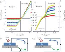
In order to further study the mechanism of the shunt effect of silicon, the I– V characteristic curve with a positive electrode connected to the substrate is also investigated. As shown in Figs. 3(a) and 3(b), each of the I– V curves shows a high unidirectional conductivity without laser illumination, and n-type and p-type junctions present opposite turn-on and turn-off state due to the opposite built-in electrical field. The IV curve in the on-state shows no obvious variation under different illumination intensities. However, the off-state leak current relies particularly on the illumination since its magnitude increases with the laser intensity. The reason for this is that the laser excites electrons in the valence band of silicon to the conducting band, leaving holes in the valence band. The photogenerated electron-hole pairs are then separated by the built-in field and stay at the metal and on the semiconductor sides, respectively. For example, in Ta/p-Si the separation of photogenerated carriers makes the film negatively-charged. When Ta is connected to the negative pole, the photocurrent fails to flow through the circuit because the power supply offers an electrical field in the opposite direction (Fig. 3(c)). However, when Ta is connected to the positive pole, the photocurrent will contribute to the circuit because the power supply offers a potential difference in the same direction. The photogenerated leak current first increases with the power voltage and is then saturated, which is due to the limited number of photo-carriers generated at specific laser intensity. The saturated leak current in the off-state increases with the intensity of laser power. Hence, we may conclude that photocurrent can (cannot) flow through the off-state junction when the film is connected to the positive (negative) electrode for p(n)-type Schottky junction.
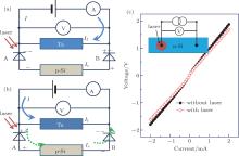
Taking Ta/p-Si as an example, the whole structure can be simplified reasonably into an equivalent electrical circuit, as shown in Fig. 4. Diodes A and B represent the Schottky contacts between the film and the substrate at the electrode position, as shown in Fig. 1(a). It can be concluded that


where If, Is, and I are the current flow in the film, the current flow in the substrate, and the bias-injected total current, respectively; Rf is the resistance of the film. We then differentiate Eq. (2) with respect to I and have

According to Eq. (3), when the current in silicon, Is, does not change with the total external current, which means dIs(I)/dI = 0, the differential resistance is constant. The decrease of resistance occurs only when

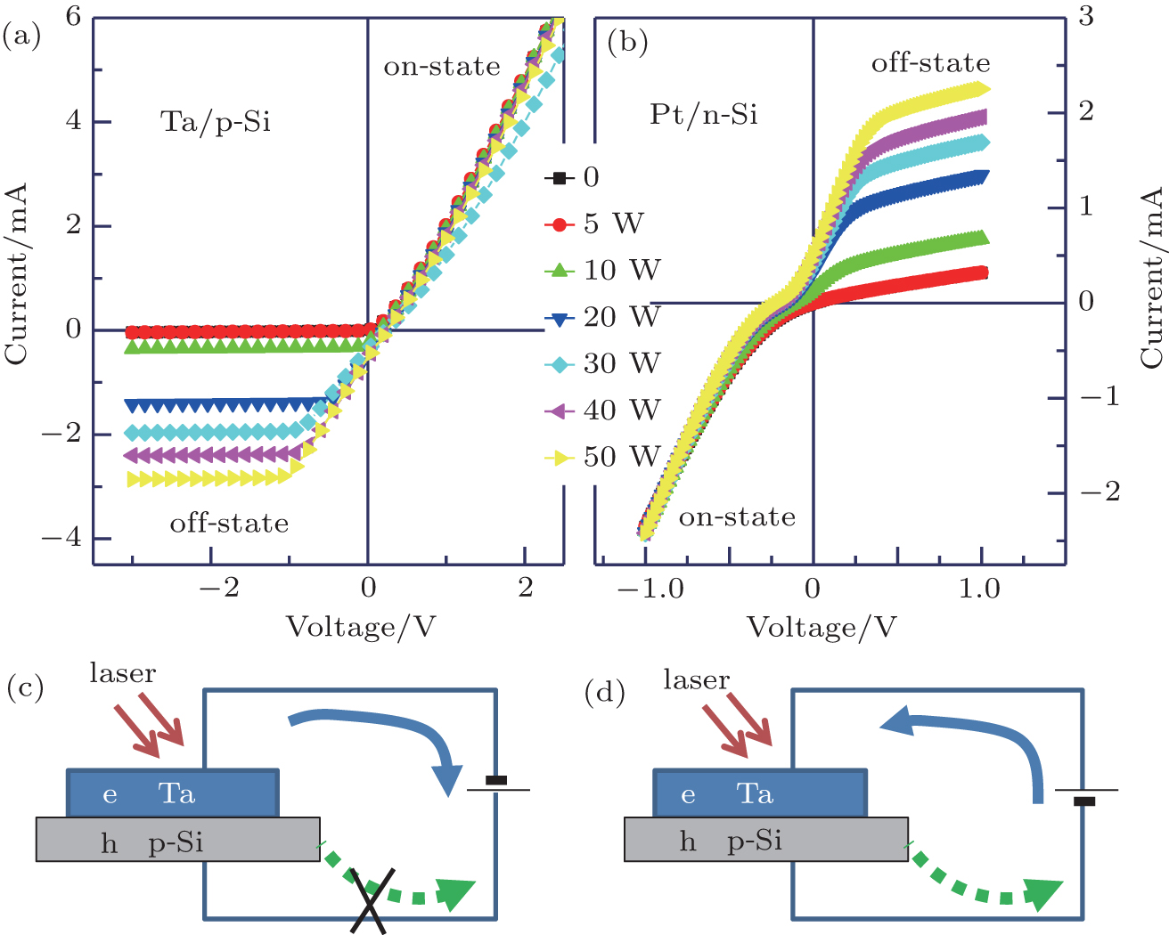 | Fig. 3. I– V characteristic curves of (a) Ta/p-Si junction and (b) t/n-Si under laser illumination at different intensities; (c) and (d) the equivalent electrical circuits when Ta is connected to the negative or positive electrode of power supply, where the solid (blue) arrow shows the injected current by external power, and the dotted (green) arrow represents the photocurrent. |
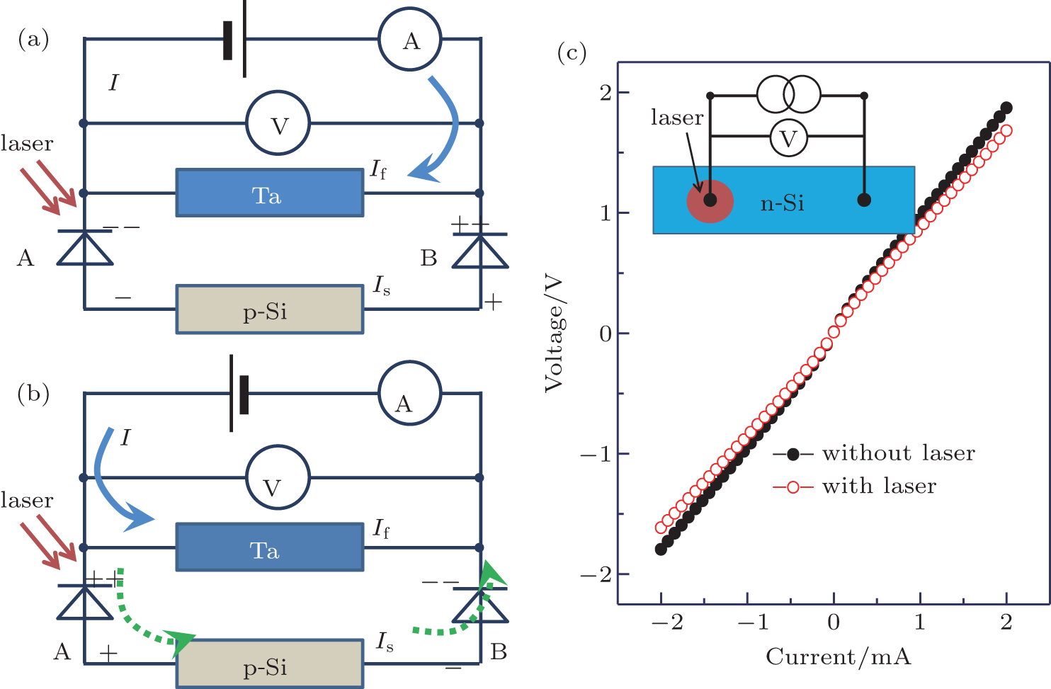 | Fig. 4. Equivalent electrical circuit simulating Ta/p-Si structure when the illumination spot is connected to the negative (a) or positive (b) pole of power supply. Solid (blue) and dotted (green) arrows represent the current injected by external power supply and the photocurrent, respectively; (c) the I– V curves in n-Si with and without the light incident on the Al/Si contact. |
When the illuminated position is connected to the negative (positive) electrode of the bias, the film at electrode A is more negatively (positively) related to the substrate (marked in Figs. 4(a) and 4(b)), so the Schottky junction A is in the on- (off-) state. When the negative electrode is connected to A, no current can pass through diode B due to the reverse cut-off property of Schottky contact, so Is basically does not change with total current and maintains zero (dIs(I)/dI ≈ 0). According to Eq. (3), differential resistance dV/dI keeps constant, corresponding to the constant region in Fig. 2. However, when the positive electrode is connected to the illuminated position, diode A is in the off-state. Under laser illumination, diode A seems to open and photocurrent can pass through the silicon as mentioned in Fig. 3. The Is increases with total current increasing and then becomes saturated (Fig. 3). In other words, the differential resistance changes with total current and then returns to the original level. According to Eq. (1), this situation corresponds to the changing region. Therefore, the shunt effect of silicon is obvious only when the proper electrode of the bias is connected to the illuminated position.
It is necessary to emphasize that the position of illumination is very important for observing the differential resistance change. When the light is incident on the Al/Si contact or on an area of bare Si, the photogenerated electrons and holes will combine with each other immediately because of the lack of an in-built electrical field to separate them. It is reported that the diffusion length of carriers in silicon is less than 0.2 mm.[16, 17] In this case, the I– V characteristics remain nearly unchanged, as shown in Fig. 4(c). The slight change is due to the contribution of photogenerated carriers to the conductivity. However, this change is center symmetric, which is not the case in Fig. 2.
The in-plane transport behavior of a Schottky junction under illumination is investigated. The lateral resistance reduction is observed by changing the direction of the injected current. The analysis of the voltage-current characteristics of the junctions under laser illumination provides further evidence for the resistance reduction induced by the light-controlled leak current. These results indicate that the change of differential resistance is strongly correlated to the shunt effect of the substrate.
| 1 |
|
| 2 |
|
| 3 |
|
| 4 |
|
| 5 |
|
| 6 |
|
| 7 |
|
| 8 |
|
| 9 |
|
| 10 |
|
| 11 |
|
| 12 |
|
| 13 |
|
| 14 |
|
| 15 |
|
| 16 |
|
| 17 |
|