Fermi level pinning effects at gate–dielectric interfaces influenced by interface state densities
[Hong Wen-Ting, Han Wei-Hua† , Lyu Qi-Feng, Wang Hao, Yang Fu-Hua]
, Lyu Qi-Feng, Wang Hao, Yang Fu-Hua]
|
|


†Corresponding author. E-mail: weihua@semi.ac.cn
*Project supported by the National Natural Science Foundation of China (Grant Nos. 61376096, 61327813, and 11234007).
The dependences of Fermi-level pinning on interface state densities for the metal–dielectric, ploycrystalline silicon–dielectric, and metal silicide–dielectric interfaces are investigated by calculating their effective work functions and their pinning factors. The Fermi-level pinning factors and effective work functions of the metal–dielectric interface are observed to be more susceptible to the increasing interface state densities, differing significantly from that of the ploycrystalline silicon–dielectric interface and the metal silicide–dielectric interface. The calculation results indicate that metal silicide gates with high-temperature resistance and low resistivity are a more promising choice for the design of gate materials in metal-oxide semiconductor (MOS) technology.
With aggressive down-scaling of complementary metal-oxide-semiconductor (CMOS) transistors, traditional polycrystalline silicon gates have been replaced by metal gates on a high-k dielectric layer to optimize the threshold voltage by reducing the gate depletion effect.[1, 2] However, the desirable effective metal work function ϕ m, eff for the metal gate remains a challenge because of stronger Fermi-level pinning effects at the metal– dielectric interface, which has been well explained by the metal-induced gap state (MIGS) model.[3] The pinning factor S is used to reflect the distortion slope of the vacuum level of the metal gate by the dielectric screening, which can be evaluated by the interface state density of the unoccupied donor-like states above the metal Fermi level Efm for a given metal– dielectric interface. Charges transfer across the metal– dielectric interface to create a dipole by these unoccupied donor-like states. The interface dipole drives the metal Fermi level toward the charge neutrality level Ecnl, d on the dielectric side to give a zero dipole charge. Consequently, the effective metal work function differs from the vacuum metal work function ϕ m, vac.
In the MIGS model, the wave functions of the electrons will decay exponentially in the dielectric layer but they will keep continuity at the metal– dielectric interface, generating intrinsic states in the band gap.[3] The pinning factor S depends on the density of interface states around the charge neutrality level of the high-k dielectric layer Ddm (Ecnl) and the width of the dipole layer δ as[4]

The parameter Ddm(Ecnl)δ is related to the electronic polarizability (ε ∞ − 1) of the high-k dielectric layer. The empirical relationship between S and (ε ∞ − 1) has been given by[5]

There are two limits: (i) the pinning factor S = 1 suggests that the effective metal work function equals metal work function in vacuum, indicating no pinning in the band gap; and, (ii) the pinning factor S = 0 indicates that the Fermi-level of the interface is strongly pinned at the charge neutrality level of the high-k dielectric layer, which can be regarded as a semiconductor with a wide band gap, [6] making the effective work function depend entirely on the characteristic of interface. Effective metal work functions on high-k dielectrics such as SiO2, Al2O3, Si3N4, ZrO2, and HfO2 are achieved to differ from their values in vacuum with the empirical model.[5, 7, 8] In fact, if the high-k dielectric is definite, then the same value of S for each metal would be determined according to the empirical model. Furthermore, the deviation between the slope of the MIGS line in metal– dielectric-semiconductor stacks and the experimental data indicates that there are other factors that influence the Fermi-level pinning effect.[9, 10] It has been observed that the Fermi-level pinning effect is also influenced by the electron state density of the metal gate induced by the image charge of the interface charge. The pinning factor S can be further calculated by the continuity of the vacuum level and charge neutralization conditions.[11] The calculation provides a more precise value of S than that in MIGS. However, there are still few results concerning the change of the electron state density and interface state density.
Although a polysilicon gate suffers gate depletion, high poly-sheet resistance, boron penetration, and other problems, the high-temperature resistant and the natural oxide layer allow the polysilicon gates to be more meaningful than metal gate in some respects. In this work, the dependences of Fermi-level pinning on interface state densities for the metal– dielectric, ploycrystalline silicon– dielectric, and metal silicide– dielectric interfaces are investigated to understand the Fermi-level pinning effects of gate– dielectric interfaces. The calculation results of the pinning factors and effective work functions of gate materials indicate that a metal silicide would be a more appropriate option for designing the gate materials in MOS technology.
When a metal connects to a high-k dielectric, the electrons of the metal gate will flow from the metal into the dielectric layer, exchanging charges with the interface states in the dielectric layer created by metal-induced gap states and external defects.[12– 15] This drives the metal Fermi-level Efm to move toward a position at the high-k dielectric so that the net dipole charge would become neutral and the system would become balanced. The position at the high-k dielectric is known as the charge neutrality level Ecnl, d.[7, 8] The equilibrium Fermi-level Efm, eff is at the position of Fermi-level pinning.
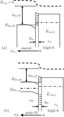
As shown in Fig. 1, a dipole will be formed at the metal– dielectric interface as a negative charge builds up on the dielectric side and an image positive charge builds up on the metal side. An electrostatic potential induced by the dipole will give rise to the deformation of the vacuum level, especially for the vacuum level of the metal Um and metal– dielectric interfacial layer Udm. The net charge density of the metal– dielectric interface ρ dm(x) is determined by the states between Ecnl, d and Efm, eff, while the image charge density of the metal ρ m(x) depends on the states between Efm and Efm, eff. The charge density is determined by the following equations:[11, 12]


where e is the elementary charge, Ddm and Dm are the interface state density of metal– dielectric interface and electron state density of the metal, respectively. As shown in Fig. 1(b), the connection of high-k dielectric with ploycrystalline silicon is similar to that of the metal with high-k dielectric. In fact, the principles of connections are derived from the semiconductor heterojunction interfaces given by Tersoff.[16] However, the critical characteristic that differentiates the ploycrystalline silicon– dielectric interface from metal– dielectric interface is the absence of interface states at the overlapping band gap.[7, 8] As the charge neutrality level in ploycrystalline silicon Ecnl, Si moves toward Ecnl, d, the net charge density ρ dSi(x) at the ploycrystalline silicon– dielectric interface is produced by the states which are induced by the alignment of Ecnl, Si and Ecnl, d as well as by the position of Fermi-level EfSi in vacuum and equilibrium Fermi-level EfSi, eff for ploycrystalline silicon, while the image charge density of ploycrystalline silicon ρ Si(x) depends on the states between EfSi and EfSi, eff. The vacuum level of ploycrystalline silicon USi and the ploycrystalline silicon– dielectric interface UdSi are continuous, the charge density is given by the following equations:[11, 12]


where DdSi and DSi are the interface state density of ploycrystalline silicon– dielectric interface and electron state density of the ploycrystalline silicon, respectively. Since the charge density ρ (x), vacuum level U, and electrostatic potential ϕ have the equations U = − eϕ and d2ϕ /dx2 = − ρ (x)/ε (ε is the permittivity of material), the equilibrium Fermi-levels can be calculated by using the boundary conditions of U(0) = 0, U(x), and dU/dx continuous at x = dm/Si (dm or dSi is the thickness of metal– dielectric or ploycrystalline silicon– dielectric interfacial layer, respectively).[12] The effective work functions ϕ m = 0 − Efm and ϕ Si, eff = 0− EfSi, eff of the metal and ploycrystalline silicon are expressed, respectively, as


in which ϕ cnl, d = 0− Ecnl, d and ϕ cnl, Si = 0− Ecnl, Si are the charge neutrality levels of the dielectric and ploycrystalline silicon with respect to the vacuum level. Consequently, the pinning factor Sm/Si of a metal or ploycrystalline silicon gate can be described by

where

and bm/Si = e2Ddm/Si/ε d are the parameters associated with materials dielectric, kd and kv/Si are the relative permittivity of the high-k and vacuum or ploycrystalline silicon, and Δ kv/Si = (kd − kv/Si) is the relative permittivity difference between the high-k and vacuum or ploycrystalline silicon.
 | Fig. 1. Schematic diagrams of the band alignment of the formed metal– dielectric and ploycrystalline silicon– dielectric gate stacks. |
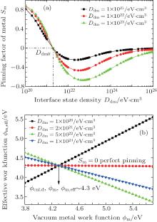
In order to obtain an insight into the role of the electron state density and the interface state density, we calculate pinning factors Sm and SSi by deriving Eq. (9) with the value of high-k dielectric Al2O3, in which the elementary charge is e ∼ 1.6 × 10− 19 C, the relative permittivity kv ∼ 1, the interface thickness dm/Si ∼ 0.25 nm, [17] the relative permittivity kd ∼ 9, and charge neutrality level ϕ cnl, d of Al2O3 ∼ 4.3 eV. Figure 2(a) demonstrates that the Fermi-level pinning and effective work function of metal are influenced largely by the density of interface states Ddm at the metal– dielectric interface and the electron state density Dm of the metal gate. With the increase of Ddm, the pinning factor Sm decreases rapidly from 1 to negative and then tends toward zero. A transition interface state density Ddm0 would make Sm ∼ 0 before perfect pinning, which only depends on the permittivity of dielectric. In the MIGS model, the Fermi-level in the interface cannot pass over the charge neutrality level, so that pinning factor Sm would not be negative.[17] However, when Ddm is greater than the transition density Ddm0, the Sm derived from our model becomes negative because of the larger relative permittivity of dielectrics than that of metals (kv ∼ 1). The negative Sm has also been observed physically on narrow gap semiconductors and experimentally on MoS2.[17, 18] Additionally, the metal with higher electron state density Dm has a larger range of Sm, implying the weaker pinning of metal work function toward ϕ cnl, d. The linear relationships between calculated effective metal work function and vacuum metal work function are illustrated in Fig. 2(b) with Dm ∼ 1023/eV· cm3 and different values of Ddm. The effective work function approximately equals vacuum work function with a small interface state density. Increasing the interface state density Ddm makes the slope of ϕ m, eff decrease positively and then increase negatively. The scope of ϕ m, eff is also reduced. This suggests that the effective metal work function will be pinned at the charge neutrality level of Al2O3 eventually, which is independent of the vacuum metal work function. This tendency is consistent with the metal pinning factor curve in Fig. 2(a). Furthermore, the intersection in Fig. 2(b) shows ϕ m, eff = ϕ m = ϕ cnl, d ∼ 4.3 eV for Al2O3, and the intersection is only influenced by the high-k dielectric layer, no matter what the change of Ddm is.
 | Fig. 2. (a) Pinning factors of metal Sm versus interface state density Ddm for different values of Dm. The large Ddm enables Sm to be pinned at zero. (b) Effective work functions versus vacuum metal work function for different values of Ddm. The smaller Sm leads to more pinning of ϕ m, eff to ϕ cnl, d, as plotted in the ϕ m, eff– ϕ m diagram. |
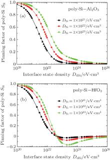
The pinning factor SSi of ploycrystalline silicon– Al2O3 is plotted as a function of DdSi and DSi in Fig. 3(a). SSi changes rapidly from 1 to 0 with the increase of the interface state density DdSi, while increasing the electron state density of ploycrystalline silicon DSi has much less influence. The effective work function of ploy-Si, ϕ Si, eff, derived by Eq. (8) should be close to ϕ Si as SSi ∼ 1. The ploycrystalline silicon-Al2O3 stack with SSi ∼ 0 would tend to pin ϕ Si, eff more effectively to ϕ cnl, Si − ϕ cnl, d + ϕ Si, which is the Fermi-level pinning position for ploycrystalline silicon. Yet for ploycrystalline silicon– HfO2 (ϕ cnl, d ∼ 4.7 eV), the more negative SSi in Fig. 3(b) shows that the curve change is similar to the metal pinning factor curve in Fig. 2(a). The reason for this is that the relative permittivity of HfO2 (kd ∼ 20) is larger than that of Si (kSi ∼ 11.9) while the relative permittivity of Al2O3 (kd ∼ 9) is smaller than that of Si.
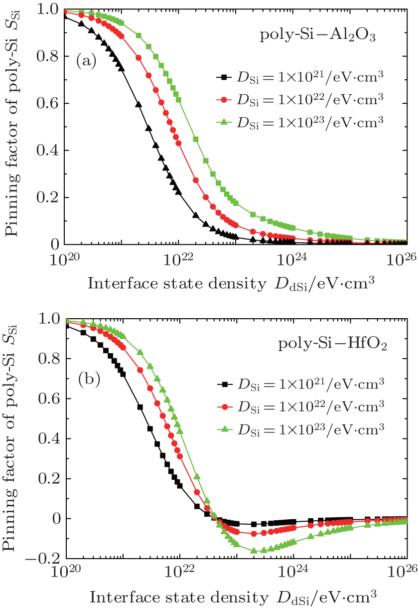 | Fig. 3. (a) Plots of semiconductor pinning factor SSi for ploycrystalline silicon– Al2O3 versus interface state density DdSi with various values of DSi. The large DdSi enables SSi to be pinned at 0. (b) Plots of pinning factor of poly-Si SSi versus interface state density DdSi. SSi for ploycrystalline silicon– HfO2 become negative with the large DdSi. |
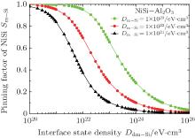
Recently, fully silicided metal silicides such as NiSi and Hf-silicide have been intensively evaluated as an alternative to metal gates due to their CMOS compatibility with polycrystalline silicon gate process and no process-induced damage to the gate dielectric. Moreover, a full silicidation gate can eliminate the ploycrystalline silicon depletion and enhance carrier mobility.[19– 21] Furthermore, the rare earth silicide gate materials have been used to reduce the Schottky barrier height because the pinning factors of rare earth silicide gates are steeper than those of the pure metal gates.[22– 24] Experimental data and ab-initio calculations have indicated that metal silicide gates such as NiSi, HfSi2, and PdSi2 have weaker Fermi level pinning than the pure metal gates.[25, 26] The pinning factor Sm− Si of NiSi– Al2O3 as a function of the interface state density Ddm− Si and electron state density Dm− Si is calculated by Eq. (9). Since the relative permittivity of NiSi (kNiSi ∼ 24.74) is larger than that of Al2O3, [26] the values of Sm− Si are positive. As shown in Fig. 4, Sm− Si changes rapidly from 1 to 0 with the increase of Ddm− Si, which is similar to the pinning factor of ploycrystalline silicon in Fig. 3(a). We can observe from Figs. 2(a), 3(a), and 4 that the values of the pinning factor for metal– Al2O3, ploycrystalline silicon– Al2O3, and NiSi– Al2O3 interfaces are ∼ 0.293, ∼ 0.940, and ∼ 0.995 respectively when Dm = DSi = Dm− Si ∼ 1023/eV· cm3 and Ddm = DdSi = Ddm− Si ∼ 1021/eV· cm3. The pinning factors of a metal gate are much smaller than those of a metal silicide gate and a ploycrystalline silicon gate, which leads to a higher degree of pinning of metal Fermi level. This also holds true for other state densities.
 | Fig. 4. Plots of pinning factor of metal silicide Sm− Si versus interface state density Dm− Si for NiSi– Al2O3 with various values of Ddm− Si. |
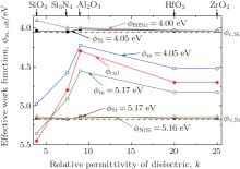
Table 1 summarises some of the basic physical parameters for dielectrics, including relative permittivity k, energy band gap Eg, electron affinity χ , the extracted (Ecnl − Ev) values, and charge neutrality level ϕ cnl measured from the vacuum level. The band gap for high-k dielectric is known from the ellipsometry and absorption data.[27, 28] The electron affinity of HfO2 is 2.4 eV from Sayan et al.[29] The extracted (Ecnl − Ev) values of Al2O3, HfO2, ZrO2 are obtained by using the tight-binding method given by Robertson.[27, 28] The extracted (Ecnl − Ev) values of Si3N4 is 2.6 eV given by Xu and Ching.[30] The charge neutrality levels of dielectrics in Table 1 are deduced from ϕ cnl = χ + Eg − (Ecnl − Ev) according to the energy band gap Eg, electron affinity χ , and the extracted (Ecnl − Ev) values. Figure 5 shows the effective work functions of these three gates on various dielectrics versus the relative permittivity of dielectrics with parameters of Table 1. It can be observed that the changes of effective work functions are compared for different metal– dielectric stacks with ϕ m = 4.05 eV, n+ ploycrystalline silicon– dielectric stacks with ϕ Si = 4.05 eV, and metal silicide– dielectric stacks with ϕ m− Si = 4.00 eV (HfSi2, k ∼ 20.56).[26] As shown in Fig. 5, the metal gate tends to pin their effective work function to ϕ cnl of the dielectrics, while the effective work functions of ploycrystalline silicon gate and metal silicide gate wave around their vacuum work functions. This implies that the metal gate is more susceptible to interface state than a ploycrystalline silicon gate or a metal silicide gate. This is also true for metal– dielectric stacks with ϕ m = 5.17 eV, p+ ploycrystalline silicon– dielectric stacks with ϕ Si = 5.17 eV, and metal silicide– dielectric stacks with ϕ m− Si = 5.16 eV (NiSi, k ∼ 24.74). Since a metal silicide gate has advantages, including high-temperature resistant and low resistivity at the same time, it would be a more appropriate option for designing gate materials in MOS technology.
| Table 1. Basic physical parameters for several dielectrics. |
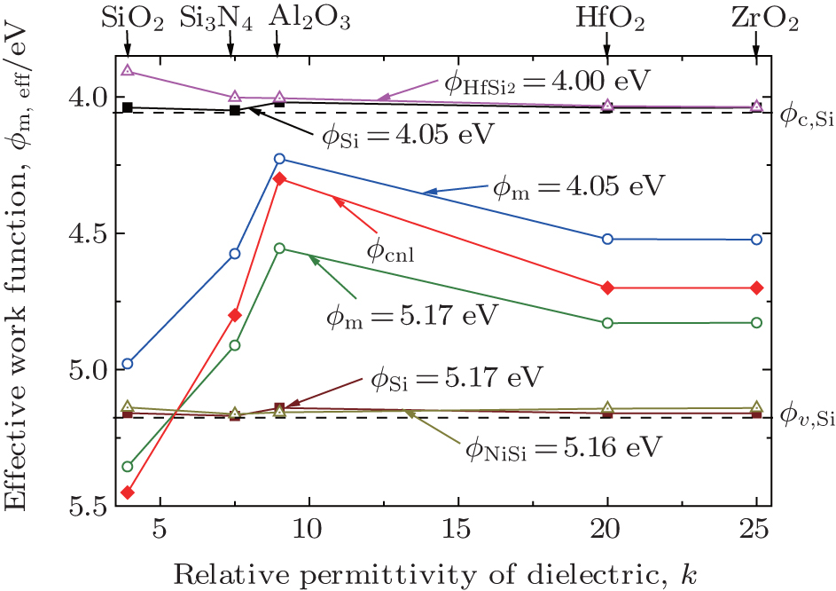 | Fig. 5. Effective work functions of ploycrystalline silicon gate, metal gate, and metal silicide gate on various dielectric layers versus the relative permittivity of dielectric with Dm = DSi ∼ 1023/eV· cm3 and Ddm = DdSi ∼ 1021/eV· cm3. |
In this paper, the dependences of the Fermi-level pinning effect on the electron state density and the interface state density are studied by comparing the metal– dielectric, ploycrystalline silicon– dielectric, and metal silicide– dielectric interfaces. The relation curves of the pinning factors with the electron state density and interface state density can reflect the Fermi-level pinning effect intuitively. The Fermi-level pinning factors and effective work functions of the metal– dielectric interfaces are observed to be significantly different, with increasing interface state density, from those of ploycrystalline silicon– dielectric interface and metal silicide– dielectric interface, implying that the metal gate is more susceptible to the interface states than a ploycrystalline silicon gate and a metal silicide gate. The calculation results indicate that a metal silicide gate would be a more appropriate option for designing the gate materials in MOS technology.
| 1 |
|
| 2 |
|
| 3 |
|
| 4 |
|
| 5 |
|
| 6 |
|
| 7 |
|
| 8 |
|
| 9 |
|
| 10 |
|
| 11 |
|
| 12 |
|
| 13 |
|
| 14 |
|
| 15 |
|
| 16 |
|
| 17 |
|
| 18 |
|
| 19 |
|
| 20 |
|
| 21 |
|
| 22 |
|
| 23 |
|
| 24 |
|
| 25 |
|
| 26 |
|
| 27 |
|
| 28 |
|
| 29 |
|
| 30 |
|