

A C-band 55% PAE high gain two-stage power amplifier based on AlGaN/GaN HEMT
[Zheng Jia-Xina) , Ma Xiao-Hua†a)  , Lu Yang
b) , Zhao Bo-Chaob) , Zhang Hong-Hea) , Zhang Menga) , Cao Meng-Yib) , Hao Yuea), b) ]
, Lu Yang|
|

 , Lu Yang
†Corresponding author. E-mail: xhma@xidian.edu.cn
*Project supported by the National Key Basic Research Program of China (Grant No. 2011CBA00606), Program for New Century Excellent Talents in University, China (Grant No. NCET-12-0915), and the National Natural Science Foundation of China (Grant No. 61334002).
A C-band high efficiency and high gain two-stage power amplifier based on AlGaN/GaN high electron mobility transistor (HEMT) is designed and measured in this paper. The input and output impedances for the optimum power-added efficiency (PAE) are determined at the fundamental and 2nd harmonic frequency ( f0 and 2 f0). The harmonic manipulation networks are designed both in the driver stage and the power stage which manipulate the second harmonic to a very low level within the operating frequency band. Then the inter-stage matching network and the output power combining network are calculated to achieve a low insertion loss. So the PAE and the power gain is greatly improved. In an operation frequency range of 5.4 GHz–5.8 GHz in CW mode, the amplifier delivers a maximum output power of 18.62 W, with a PAE of 55.15% and an associated power gain of 28.7 dB, which is an outstanding performance.
Gallium nitride (GaN) is the third generation semiconductor material with the advantages of wide band-gap, high breakdown voltage and high electron saturate drift velocity. GaN device can operate in severe environment because of its superior temperature and radiation performance.[1, 2] Amplifiers, transmitter/receiver T/R modules and radars based on GaN devices are less complex, with output power density, gain, efficiency and reliability improved.[3– 6] In recent years, many two-stage power amplifiers based on GaN HEMT have been reported. Although they have achieved splendid performances, the power added efficiency PAE is less than 50% and the associated power gain is less than 25 dB.
In this paper, a C-band two-stage power amplifier based on the GaN HEMT is designed with a high PAE of 55.15% and the associated power gain of up to 28.7 dB. The harmonic manipulation networks are designed matching the impedances to the optimum input and output impedances at f0 and 2f0 based on the load-pull results, [7– 10] and the inter-stage power divider and the output power combiner transition networks are designed and optimized to obtain a low impedance transformation ratio and a low insertion loss, so the PAE and the power gain are significantly increased. In an operation frequency range of 5.4 GHz– 5.8 GHz in CW mode, the amplifier delivers a maximum output power of 18.62 W, with a PAE of 55.15% and an associated power gain of 28.7 dB, which is an outstanding performance.
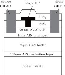
The AlGaN/GaN HEMT used in this paper was developed in Xidian University. Figure 1 shows the cross section of the device with a total gate width of 10 mm × 0.125 mm. The undoped AlGaN/AlN/GaN heterostructure layers were grown on a 2-inch (1 inch = 2.54 cm) 4H– SiC substrate by metal-organic chemical vapor deposition. An AlN nucleation layer of 100 nm in thickness was deposited on an SiC substrate. Then a 2-μ m-thick GaN buffer layer was grown, followed by a 1-nm interlayer and a 20-nm-thick undoped AlGaN barrier layer. At room temperature, the sheet resistance is approximately 320 Ω /◻ . The sheet carrier density and the electron mobility are 1.3 × 1013 cm− 2 and 2050 cm2/(V· s), respectively. Isolation was accomplished by Cl2-based dry etching with a depth of 150 nm. Ti/Al/Ni/Au source and drain Ohmic contacts (OHMC) were formed by electron-beam evaporation and annealed at 870 ° C for 30 s. Then SiN passivation was achieved with plasma-enhanced chemical vapor deposition (PECVD) with a thickness of 60 nm. The gate recess was performed by plasma etching. The gate footprint with the Lg of 0.25 μ m was opened by etching SiN using CF4 plasma. After the gate photolithography, the Schottky gate was formed by Ni/Au/Ni. The gate electrode overlapped the SiN layer, forming a T-type field-plate (FP) structure.[11, 12] Finally, SiN passivation layer was deposited by PECVD to protect the device. The detailed grown epitaxy and device process had been described in Ref. [13]. The saturation current density of the device was 1.6 A/mm at Vgs = 1 V and the peak transconductance was 650 mS/mm at 10 V drain bias. The threshold voltage was about − 2.7 V.
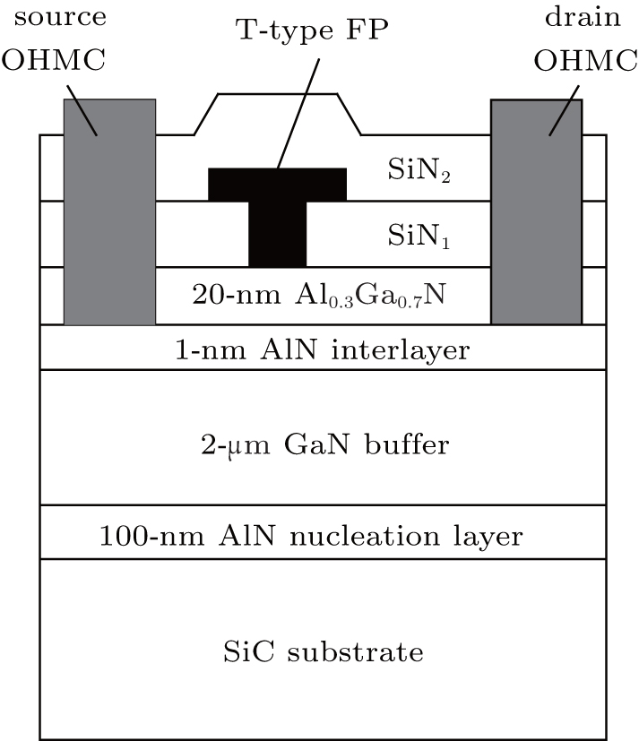 | Fig. 1. Cross section of an AlGaN/GaN HEMT. |
The impedances for the optimum PAE of a 1.25-mm AlGaN/GaN HEMT are determined by the load-pull and source-pull systems each composed of a vector network analyzer, a probe station and tuner. As Table 1 shows, for example, at 5.6 GHz, the optimum source impedances at f0 and 2f0 are (1.738 + j2.205) Ω and (0.712 − j5.038) Ω , respectively, and the optimum load impedances at the f0 and 2f0 are (8.484 + j19.110) Ω and (4.525 + j15.023) Ω , respectively.
| Table 1. Optimum source and load impedances. |
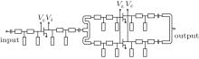
The schematic and layout were designed and simulated in ADS and HFSS. The large signal model was established based on the EEHEMT model by IC-CAP software.[14, 15] Multi-stage microstrip is designed in both input and output serving as the 2nd harmonic manipulation network to tune the 2nd harmonic as shown in Fig. 2. In the output matching network, two open stubs are designed: one is near the HEMT, manipulating the 2nd harmonic (That 2nd harmonic manipulation structure can also be microstrip on high permittivity material.), and the other matches the output impedance at f0. At the input, harmonic manipulation network is also adopted. With the design of 2nd harmonic manipulation network, the impedance at 2f0 is matched to the optimum point.
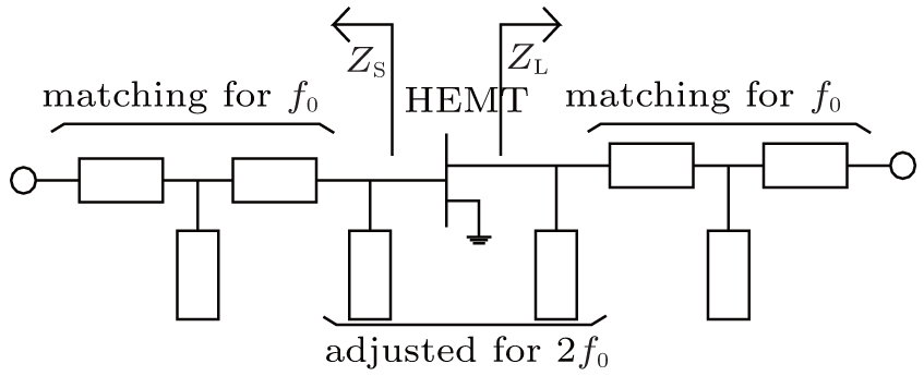 | Fig. 2. The 2nd harmonic manipulation network. |
Then, the effect of 2nd harmonic impedance mismatch on the PAE is explored at f0 = 5.6 GHz. The results are listed in Table 2. First, at a fixed ZL = 4.525 + j15.023 Ω @2f0, ZS@2f0 varies in a circle which centers at (0.712 − j5.038) Ω on the Smith chart and the PAE varies from 51.08% to 60%. Next, at a fixed ZS = 0.712 − j5.038 Ω @2f0, ZL@2f0 varies in a circle which is centred at (4.525 + j15.023) Ω and the PAE varies from 50.22% to 60%. The variation of the PAE with the 2nd harmonic impedance demonstrates that the mismatch of the 2nd harmonic impedance will deteriorate the PAE significantly.
| Table 2. The 2nd harmonic impedances dependence of maximum PAE. |
The circuit is designed as a two-stage amplifier with a staging ratio of 1:4. The power stage comprises two 2.5-mm cells, resulting in a total gate width of 5 mm. According to the measured impedances of 1.25-mm HEMT, the optimum impedances for 2.5-mm HEMT at f0 and 2f0 can be scaled and calculated. Multi-stage microstrip matching networks are designed at both the input and the output of the amplifier stage, serving as the 2nd harmonic manipulation networks.
The driver stage and the power stage are connected by the inter-stage Wilkinson power divider. The output and inter-stage networks have been designed and optimized to present impedances determined at the transistor gate port and drain port. First, the output impedance of the driver stage is matched to 30 Ω , and the input of the amplifier stage to 20 Ω , so the impedance of the divider is calculated from the following equation:

where Z0 is the impedance of the divider, Z1 and Z2 are the impedances of the input and the output, respectively. So the impedance is calculated and optimized to 35.93 Ω . The output network of the power stage is a Wilkinson power combiner whose impedance is 30 Ω . The block diagram of the two-stage amplifier is shown in Fig. 3.
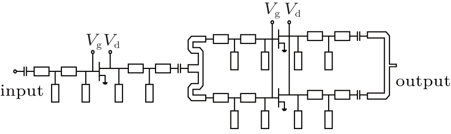 | Fig. 3. Block diagram of the two-stage amplifier. |
A resistor is set at the gate bias network to make the stable factor K > 1.2, which meets the absolutely stable condition. Capacitors are set at the input and output to block the DC. The capacitors in the bias network can decouple the noise from DC. The quarter wavelength microstrips are used to block the RF signal.
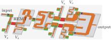
Figure 4 shows the 3D model and the test system of the amplifier. The microstrip circuits were manufactured on the Alumina with a relative permittivity of 9.8. The size of the amplifier module is 8 mm × 16 mm. The amplifier module was soldered on a rectangular carrier which was fixed on the fixture by four screws. The 1 μ F capacitors on the carriers can decouple the noise from the DC power source and supply path for the DC voltage from the DC supplier to the gate and drain. Alumina 50-Ω microstrip lines were connected to the RF ports of the amplifier with bonding wires. The far ends of the 50-Ω lines were connected with connectors which could be calibrated from the measurements.
 | Fig. 4. 3D model of the amplifier. |
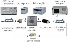
In the test system in Fig. 5, an Agilent E4419B two-channel power meter is used to detect the input and output power simultaneously. The harmonic distortion performance is studied by an Agilent E4447A spectrum analyzer. An aluminum heat sink accompanied by a fan is used to keep the amplifier operating at a moderate temperature.
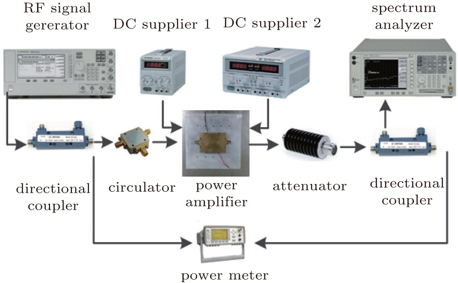 | Fig. 5. Test system for the amplifier. |
The microwave performance of the amplifier is measured under the bias condition of Vdsq = 28 V and Idsq = 500 mA. When RF signal is applied, Ids varies from 1.1 A to 1.3 A, and DC power consumption is in a range from 30.8 W to 36.4 W. Figure 6(a) shows the variations of output power, gain, and PAE with input power at 5.6 GHz. When the input power is 14 dBm, a PAE of 55.15% is obtained, the output power is 18.62 W (42.7 dBm), and the associated power gain is 28.7 dB, with 3dB compressed compared with a small signal gain of 31.7 dB, which is an outstanding performance for the two-stage GaN power amplifier. Figure 6(b) shows the variations of output power, gain and PAE with frequency. In an operation frequency range from 5.4 GHz to 5.8 GHz, the amplifier exhibits the highest PAE of 55.15% at 5.6 GHz, a maximum output power of 18.62 W (42.7 dBm), and an associated power gain of 28.7 dB. In the frequency band of 5.4 GHz– 5.8 GHz, the PAE is > 48%, the output power is > 15.5 W (41.92 dBm), and the gain flatness is 0.78 dB. So the amplifier exhibits broadband property.
 | Fig. 6. Measured (line) and simulated (dot) microwave performances of the amplifier @5.6 GHz (a) and in a frequency range from 5.4 GHz to 5.8 GHz (b). |
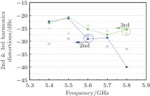
Figure 7 shows the variations of the 2nd and 3rd harmonic distortions with frequency. The 2nd harmonic is significantly suppressed by designings the 2nd harmonic manipulation network. The 2nd and 3rd harmonic distortions in the frequency range of 5.4 GHz– 5.8 GHz are both < − 20 dBc.
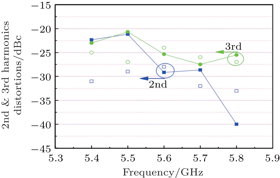 | Fig. 7. Measured (line) and simulated (dot) 2nd & 3rd harmonic distortions versus frequency. |
Moreover, the stimulated and measured performances are in agreement with each other except a discrepancy between the simulated small signal gain (33 dB) and the measured one (31.7 dB). There are some possible reasons for the distinction. First, the error introduced by the model establishment based on the measured data can make a difference with respect to the accuracy of the model. Then the discontinuity connected by the golden bonding wire containing parasitic effects introduces inserted loss. Those two points result in the disagreement between the simulated and measured results.
Listed in Table 3 are the performances of two-stage GaN amplifier ever reported. The amplifier in this paper has an outstanding performance of PAE and associated power gain compared with them, but to some extent, this is at the expense of the output power.
| Table 3. State-of-art PAE and power gain for C band two-stage GaN amplifiers ever reported. |
A high PAE high gain two-stage amplifier based on AlGaN/GaN HEMT is designed and measured in this paper. The impedances at f0 and 2f0 are matched to the optimum points for PAE by designing the 2nd harmonic manipulation network. The power divider and combiner are calculated and optimized accurately to promote the PAE and power gain. The amplifier is measured in CW mode in a frequency range of 5.4 GHz– 5.8 GHz. The maximum output power is 18.62 W, with a PAE of 55.15% and an associated power gain of 28.7 dB, indicating an outstanding performance. The 2nd and 3rd harmonic distortions are < − 20 dBc.
The authors wish to thank all the other members of the Key Laboratory of Wide Band-Gap Semiconductor Material and Devices involved in this work for their kind assistance.
| 1 |
|
| 2 |
|
| 3 |
|
| 4 |
|
| 5 |
|
| 6 |
|
| 7 |
|
| 8 |
|
| 9 |
|
| 10 |
|
| 11 |
|
| 12 |
|
| 13 |
|
| 14 |
|
| 15 |
|
| 16 |
|
| 17 | [Cited within:1] |
| 18 |
|
| 19 | [Cited within:1] |
| 20 |
|
| 21 |
|