
Rectification and electroluminescence of nanostructured GaN/Si heterojunction based on silicon nanoporous pillar array
[Wang Xiao-Boa), b) , Li Yongc) , Yan Ling-Linga) , Li Xin-Jian†a)  ]
]
]
|
|


†Corresponding author. E-mail: lixj@zzu.edu.cn
*Project supported by the National Natural Science Foundation of China (Grant No. 61176044).
A GaN/Si nanoheterojunction is prepared through growing GaN nanocrystallites (nc-GaN) on a silicon nanoporous pillar array (Si-NPA) by a chemical vapor deposition (CVD) technique at a relatively low temperature. The average size of nc-GaN is determined to be ∼10 nm. The spectral measurements disclose that the photoluminescence (PL) from GaN/Si-NPA is composed of an ultraviolet (UV) band and a broad band spanned from UV to red region, with the feature that the latter band is similar to that of electroluminescence (EL). The electron transition from the energy levels of conduction band and, or, shallow donors to that of deep acceptors of GaN is indicated to be responsible for both the broad-band PL and the EL luminescence. A study of the I– V characteristic shows that at a low forward bias, the current across the heterojunction is contact-limited while at a high forward bias it is bulk-limited, which follows the thermionic emission model and space-charge-limited current (SCLC) model, respectively. The bandgap offset analysis indicates that the carrier transport is dominated by electron injection from n-GaN into the p-Si-NPA, and the EL starts to appear only when holes begin to be injected from Si-NPA into GaN with biases higher than a threshold voltage.
A number of breakthroughs on growing and doping techniques were achieved in the 1990s, since then gallium nitride (GaN), and its ternary and quaternary alloys have become a group of most promising semiconductors that show promise in a variety of industrial fields, such as light-emitting diodes (LEDs), [1, 2] laser diodes (LDs), [3, 4] ultraviolet (UV) detectors, [5] chemical sensors, [6] high electron mobility transistors (HEMTs), [7] and solar cells.[8] In particular, they are thought to be promising materials for fabricating efficient light-emitters in the UV and visible spectral range due to their tunable direct bandgap and insensitivity to dislocations.[9] On the other hand, silicon (Si) has long been the most important semiconductor and it is widely used in the modern electronic industry because of its technical maturity, element abundance and low prices. Nevertheless Si is basically a semiconductor with an indirect bandgap, and this feature makes it an inefficient light-emitting material. Therefore, the integration of GaN with Si, which may have the potential to combine the merits of the two materials, might lead to superior or novel functionalities.[10] Based on this consideration, several approaches (such as the wafer-bonding and epitaxy-growth methods) have been developed to realize the heterogeneous integration of GaN with Si.[11] Nevertheless, the large lattice and thermal mismatch between crystal GaN and Si is a huge obstacle, and a layer of metal alloy bonding material or aluminum nitride (AlN) buffer is usually required for strong bonding[12] or high-quality GaN films.[13] Obviously, the introduction of intermediate layers makes it difficult or even impossible to use Si as a functional substrate in Si-based GaN.
Another way to realize the integration of GaN with Si is to use nanotechnology, which is becoming a promising route to integrating the highly mismatched materials through a specific stress-relaxing mode.[14] As has been illustrated by other groups, [15, 16] repeatable rectification effect was observed in GaN/Si heterojunctions prepared by growing GaN nanonods or nanowires on single crystal Si (sc-Si) substrates. Prototype devices for solar cells[17, 18] and UV detectors[19] have been demonstrated based on this material. In our previous study, [20] we reported the preparation of Si nanoporous pillar array (Si-NPA), which is a Si hierarchical structure characterized by a regular array of micron-sized, quasi-identical, and nanoporous silicon pillars with pore walls composed of Si nanocrystallites (nc-Si) encapsulated by amorphous Si oxide. The structural features of the patterned surface morphology, nanoporous structure and massive nc-Si, together with the physical properties of huge specific surface area, low light reflectance, and strong photoluminescence (PL), make Si-NPA a functional substrate for assembling various Si-based nanostructures. Through depositing foreign materials on Si-NPA, a series of prototype devices have been developed for use in gas sensing, [21] field emission, [22] surface enhanced Raman scattering, [23] and photovoltaic effect.[24] An unconventional GaN/Si heterojunction was also prepared by growing GaN nanograin thin film on Si-NPA, [25] which could give yellow or near infrared (NIR) electroluminescence (EL) under different forward bias voltages. These experimental results predict the possibility of fabricating LEDs directly based on GaN/Si nanoheterojunctions. Nevertheless, as a prototype LED, there is still large room for improving the performance of these devices, which will depend on our understanding of the underlying physics and capability in manipulating the properties of GaN/Si-NPA.
In the present paper, we report the study of a GaN/Si heterojunction prepared through growing GaN nanocrystallites (nc-GaN) on Si-NPA by a chemical vapor deposition (CVD) method at 800 ° C, which is a relatively low growing temperature compared with the previous experiments.[25] The average size of nc-GaN is evaluated to be ∼ 10 nm. The structure and morphology of GaN/Si-NPA are characterized by x-ray diffraction (XRD), field emission scanning electron microscope (FESEM), and transmission electron microscope (TEM). The electrical and luminescent properties are studied by measuring its I– V curve and PL/EL spectrum. It is shown that NIR emission originating from the interface states[25] would not appear for samples prepared at low growing temperature. Based on the experimental data, a theoretical model of the mechanism of carrier transport across the heterojunction and the origin of EL is proposed. Our study may provide an insight into the basic physics about the heterogeneous contact of GaN/Si-NPA and may be an efficient route to realizing the direct integration of GaN with Si.
Si-NPA was prepared through hydrothermally etching boron-doped, (111)-orientated sc-Si wafers in an aqueous solution of hydrofluoric acid (13 mol/l) containing ferric nitrate (0.04 mol/l), and the experiment was performed at 140 ° C for 30 min.[20] One side of Si-NPA was chemically polished with saturated sodium hydroxide solution to expose the sc-Si underneath. A thin layer of platinum (Pt, ∼ 20 nm) as catalyst was deposited on the other side of Si-NPA by using an ion spluttering apparatus (JEOL JFC-1600). Then, the Si-NPA substrate with Pt layer was loaded in a horizontal tube furnace and a quartz crucible containing 1 gram of metal gallium (Ga) as Ga source was placed 4 cm upstream from the substrate. The growth of GaN was accomplished by the chemical reaction between Ga vapor and ammonia gas at 800 ° C for 50 min. The ammonia gas flow rate was set to be 5 sccm and the inner pressure of the tube furnace was maintained at 500 Pa. Argon was inlet as a protection gas in the ramping and cooling process, and was shut down during the growing process. Afterwards a thin layer of aluminum with a thickness of 500 nm was deposited on sc-Si side as positive electrode by vacuum evaporation technique, and a thin layer of indium tin oxide (ITO) with a thickness of ∼ 100 nm was deposited on GaN side by magnetron spluttering technique as a transparent negative electrode. The final device structure is of ITO/GaN/Si-NPA/sc-Si/Al. To test the nature of the contact between ITO and GaN, two coplanar square-shape electrodes which were composed of Al and ITO, respectively, were deposited on GaN/Si-NPA. The dimensions of the electrode were 0.5 cm by 0.5 cm, and the separation between the two electrodes was 0.3 cm.
The crystal structure and surface morphology of GaN/Si-NPA were characterized by XRD (PA National X′ Pert Pro), FESEM (JSM 6700F) and TEM (JEM 2100). The PL spectrum of GaN/Si-NPA was tested using a fluorescence spectrophotometer (Horiba FL-322) equipped with a 450 W xenon lamp as the UV light source. The EL spectra of the device were measured using the same fluorescence spectrophotometer with a direct current source as the driving power. The I– V characteristic was measured through a Keithley source meter 2400. All of these measurements were carried out at room temperature.
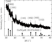
Figure 1 shows the XRD pattern of as-prepared GaN/Si-NPA for EL, where the marked peaks can be well identified and indexed to those of wurtzite GaN. The peaks located at ∼ 32.59° , 34.32° , 36.81° , 48.31° , 57.89° , 62.83° , and 69.15° are indexed to the reflections from the (100), (002), (101), (110), (102), (103), and (112) lattice family planes of hexagonal GaN, respectively. Through a simple Gaussian fitting process, the full width at half maximum (FWHM) for the first three diffraction peaks are determined to be ∼ 0.87° , 0.80° , and 0.95° , respectively. Based on the XRD data of the three diffraction peaks and using Scherrer’ s formula, the average grain size of nc-GaN is evaluated to be ∼ 10 nm. In addition to the peaks from hexagonal GaN, two other diffraction peaks are observed to be located at ∼ 41.19° and 45.17° , respectively. Judging from the peak locations and the growing process of GaN, the two diffraction peaks might originate from the reflections of Pt– Ga alloys but it is difficult to determine the accurate crystal phase and component ratio in the present experiment because there might be present a variety of stoichiometric phases in Ga– Pt compound, [26] and many of them can show diffraction peaks near the two angles. So we tend to think that the diffraction originates from some kinds of non-stoichiometric Pt– Ga alloys, which provides the foundation for the vapor-liquid-solid growing mode known in CVD process.[27]
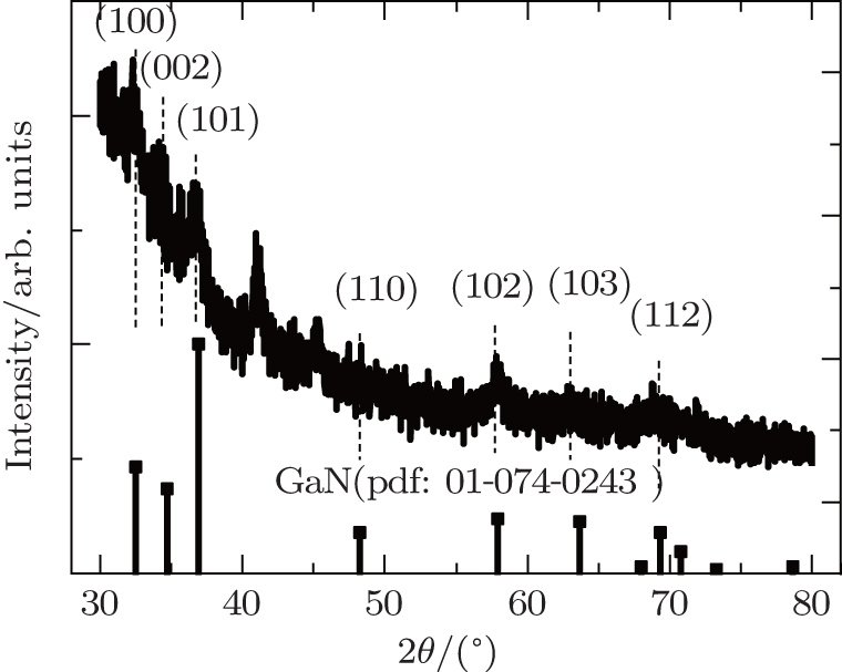 | Fig. 1. XRD spectrum of GaN/Si-NPA. |
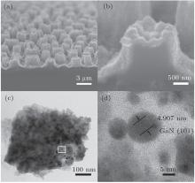
Figures 2(a) and 2(b) show the integral surface morphology of GaN/Si-NPA and that of an individual pillar obtained by FESEM, respectively. Apparently, after CVD deposition a thin layer of GaN was grown on Si-NPA, which covered both the pillars and the valleys surrounding the pillars, but the sample maintains the morphological feature of a quasi-regular pillar array similar to that of Si-NPA. Judging from the magnified image of an individual pillar (Fig. 2(b)), the thickness of the deposited GaN film is estimated to be ∼ 100 nm. To build up a direct picture of the microstructure of GaN, the experiments of TEM and high-resolution TEM are conducted by cleaving the upper layer material from GaN/Si-NPA. As shown in Fig. 2(c), two kinds of featured zones can be distinguished by comparing the image contrast, large quantities of dot-liked dark zones, and a sponge-like shallow-color matrix. Obviously, the dark zone sizes range from several nanometers to ∼ 20 nm and disperse uniformly over the shallow-color matrix. The high-resolution TEM observation is performed by taking the image of a typical dark dot noted in Fig. 2(c). As shown in Fig. 2(d), a set of lattice fringes are clearly observed. The fringe separation is determined to be ∼ 0.245 nm, which is obtained by measuring the distance across 20 fringes and is in accordance with the identity distance of the (101) lattice family planes of wurtzite GaN. This directly proves that as-deposited GaN in GaN/Si-NPA is in the form of nc-GaN. Furthermore, the grain size is measured to be ∼ 13.3 nm, which is well consistent with the average grain size (∼ 10 nm) calculated from the XRD data.
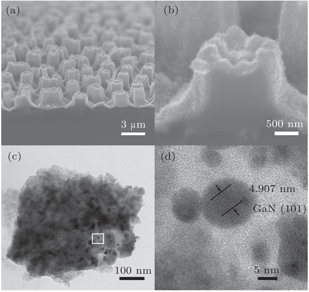 | Fig. 2. FESEM images of (a) GaN/Si-NPA and (b) an individual pillar of GaN/Si-NPA taken by tilting the sample at an angle of 60° . (c) TEM image of a piece of GaN/Si-NPA cleaved from the upper layer of a sample and (d) high-resolution TEM image of the marked region in panel (c). |
Figure 3 shows the PL and EL spectra of as-grown GaN/Si-NPA measured at room temperature. The PL spectrum of GaN/Si-NPA can be decomposed into two bands; i.e., an UV band and a broad band ranging from ∼ 300 nm– 800 nm. The peak positions and the corresponding FWHMs of the two PL bands are determined to be ∼ 381 nm and ∼ 58 nm, and ∼ 522 nm and ∼ 150 nm, respectively. Based on the feature parameters, the former could be assigned to the near band edge emission of GaN, and the latter to the radiative transition from the energy levels of conduction band and, or, shallow donors to those of deep acceptors.[28] The relatively big FWHMs for the two bands compared with the bulk GaN are most likely to be due to the broad size distribution and strong electron-phonon coupling of nc-GaN.[29] Although the exact assignment of the defects related to the broad PL band is difficult because a variety of defects can contribute to it, it is generally accepted that the deep acceptors responsible for the phenomenon are mainly the Ga vacancy and their complexes.[28] The EL spectra of GaN/Si-NPA measured at different forward biases are shown in Fig. 3(b). The EL emission is observed when the forward bias is over 5 V and the EL intensity increases rapidly with increasing forward bias. The EL spectrum has a broad and almost Gaussian peak, spanned from ∼ 300 nm to 800 nm. The peak position and FWHM are measured to be ∼ 540 nm and ∼ 155 nm, respectively. By comparing the spectral features, it is found that the FWHMs are almost identical, ∼ 150 nm and ∼ 155 nm for the PL band and EL band, respectively, but the peak position changes from ∼ 522 nm to ∼ 540 nm. The difference between the peak positions of PL and EL bands should originate from the variation of the emission sites; i.e., the upper layer GaN for PL and the bottom layer GaN (near the space charge region of GaN/Si-NPA). The spectral similarity suggests that EL has the same origin as the broad PL band; namely, the radiative transition from the energy levels of conduction band and, or, shallow donors to those of deep acceptors. By comparing with the results in Ref. [25], where GaN is grown at a high temperature of 1025 ° C, no NIR EL due to radiative recombination occurring at the interface between GaN and Si-NPA is observed. The disappearance of NIR EL should be due to the high-density defects introduced by the low-temperature CVD growing process.
 | Fig. 3. (a) PL spectrum of GaN/Si-NPA with an excitation wavelength of 270 nm and a long-pass filter centered at 320 nm used. (b) EL spectra of GaN/Si-NPA. |
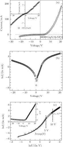
Figure 4(a) shows the I– V curve of GaN/Si-NPA, measured with a device structure of ITO/GaN/Si-NPA/sc-Si/Al. Here, an apparent rectifying effect is observed, with a turn-on voltage of ∼ 4 V, a breakdown voltage of ∼ 15 V, and a rectifying ratio of ∼ 16.8 at ± 15 V. Under a bias of + 15 V, a forward current of ∼ 85 mA is obtained with an effective junction area of ∼ 1 cm2. Deduced from the device configuration, four hetero-contacts are altogether formed in the device (i.e., the contacts between ITO electrode and GaN, GaN and Si-NPA, Si-NPA and sc-Si, and sc-Si and Al electrode) and the potential barrier existing at any of the hetero-contacts may contribute to the rectifying effect. Nevertheless, the contact between Al and heavily-doped sc-Si and that between sc-Si and Si-NPA have already been proved to be ohmic and would not contribute to the rectifying effect.[30] Theoretically Schottky contacts might be formed between ITO and p-GaN or n-GaN[31] due to its intermediate work function (∼ 4.3 eV– 4.8 eV, depending on preparation conditions[32]) between p-GaN (∼ 7.5 eV) and n-GaN (∼ 4.1 eV). Nevertheless, the Schottky barriers between ITO and n-GaN are usually very low and are often treated as Ohmic contacts, especially for n-GaN with high interface state density or high doping level.[33] To test the contact feature between ITO and as-grown GaN, a pair of coplanar electrodes (i.e., an Al electrode and an ITO electrode) are deposited on GaN/Si-NPA, and the I– V characteristic is measured, which is shown in the inset of Fig. 4(a). Here, an almost linear relation is obtained. Because the contact between Al and n-GaN has been proven to be Ohmic, [34] the result indicates that an ohmic contact is formed between n-GaN and ITO. Considering the fact that the electricity of Si-NPA is of p-type conduction[30] and that of unintentionally doped GaN is of n-type conduction, [28] the rectifying effect observed from ITO/GaN/Si-NPA/sc-Si/Al could be attributed only to the hetero-contact formed between n-GaN and p-Si-NPA.
 | Fig. 4. (a) I– V curve of GaN/Si-NPA. Inset: I– V curve of a coplanar Al/GaN/ITO structure. (b) Semilogarithm plot of I– V curve of GaN/Si-NPA. (c) Logarithm– logarithm plot of I– V curve of GaN/Si-NPA under forward bias. Inset: I/V– V plot of I– V curve of GaN/Si-NPA. |
Theoretically, the I– V characteristic curve for a heterojunction could be described by the thermionic emission theory, which states[35]

where Is is the saturation current, Rs is the series resistance, η is the ideal factor, k is the Boltzmann constant, and T is the absolute temperature. Under usual bias, the 1 in the bracket can be ignored, and with small current the effect of the series resistance can also be ignored. This would lead to the approximate relation, as follows:

To investigate the nature of the I– V characteristic of GaN/Si-NPA, the semi-logarithm plot of its I– V curve is presented in Fig. 4(b). When the forward voltage is less than 5 V, the curve is almost a straight line and the I– V shows a linear relation. This means that in the voltage range the current increases exponentially as voltage increases, which is consistent with the thermionic emission model. Through fitting the data by Eq. (2), the ideal factor of GaN/Si-NPA is evaluated to be 31.2± 0.2. Obviously, such an ideal factor is very high compared with that of n-GaN/p-Si contact (∼ 3.4), [15, 16] which might be caused by the high-density interface states between GaN and Si-NPA. As is well known, Si-NPA has a huge specific area due to its rough morphology constructed by a regular array of nanoporous Si pillars. This leads to the fact that a huge contact area is formed between GaN and Si-NPA, and the resulting high-density interface states would play a more pronounced role in as-grown GaN/Si-NPA heterojunction than in traditional planar-structured GaN/Si heterojunctions.
To further exploit the forward transport mechanism of as-prepared GaN/Si-NPA, a logarithm-logarithm plot of the I– V curve under forward bias is shown in Fig. 4(c). As shown in the figure, the ln I shows an exponential increase with lnV when the voltage is less than 5 V, and approaches to a linear region when the voltage exceeds 10 V. The fitting analysis within the linear region gives an I– V relation of I = V2.4, which is the typical indication of a space-charge-limited current (SCLC) mechanism.[36] The SCLC mechanism usually operates in wide bandgap semiconductors, insulators, and polymers due to their low intrinsic carrier concentrations when the injected carrier concentration exceeds its equilibrium value and controls the space charge and electric field profile. In ideal cases, the space charge is determined solely by the injected carrier and the I– V characteristic gives rise to a quadratic relation if the electric field is low so that the drift velocity is proportional to the electric field. For an actual material, the existence of charge traps causes the deviation from quadratic relation because they contribute only to space charge but not current. Especially, in the case of a shallow trap situation, the I– V relation is still quadratic because the ratio between free charge and total space charge is independent of voltage. In GaN/Si-NPA, that the fitted exponent (2.4) is close to 2 indicates the possibility of shallow trap SCLC mechanism, while the deviation might be brought by the potential drop across the heterojunction. To test and verify the hypothesis, the curve of I/V versus V is plotted in the inset of Fig. 4(c). As can be seen, a linear relation appears when the voltage exceeds ∼ 5.0 V. This indicates the existence of a relation of I ∝ (V − V0)2, where V0 is the voltage drop across the heterojunction.
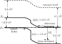
To build up a clear picture about the physical processes discussed above, the energy band diagram of GaN/Si-NPA is portrayed in Fig. 5. According to the results reported previously, the electron affinity (χ (Si-NPA)) and the bandgap (Eg (Si-NPA)) of Si-NPA are ∼ 3.6 eV and ∼ 2.0 eV, respectively.[25] The affinity (χ (GaN)) and bandgap (Eg (GaN)) of n-GaN are ∼ 4.1 eV[37] and ∼ 3.4 eV, respectively.[28] So the conduction band offset is Δ EC = χ (GaN) − χ (Si − NPA) = 0.5 eV, and the valence band offset is Δ EV = Δ EC − (Eg(Si − NPA) − Eg(GaN)) = 1.9 eV. Obviously, Δ EV is much larger than Δ EC, which indicates that the electron injection from n-GaN into p-Si-NPA will dominate the electrical transport process.
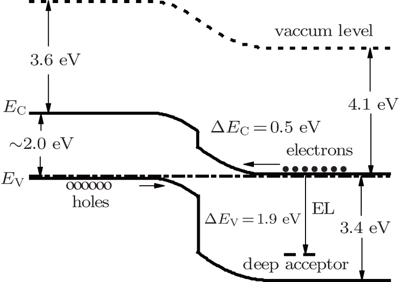 | Fig. 5. Schematic band diagram of GaN/Si-NPA. |
At a relatively low forward bias, the electrons flow from GaN to Si-NPA and then recombine with the holes therein, and give rise to the forward current. On the other hand, the flow of holes from Si-NPA to GaN is negligible due to the large energy barrier formed at the interface. As the forward bias increases, the energy barriers for both for electrons and holes would be lowered. This makes the electron flow keep on increasing rapidly, and at the same time the hole injection from Si-NPA to GaN starts when the energy barrier for the holes is lowered to a certain level. Although the holes need to get across a larger energy barrier than the electrons, a certain number of holes could be still injected into GaN when the forward bias is high enough (> 5 V). The injected holes trapped by deep acceptors in GaN would cause the hole concentration to increase as minority carriers, and finally lead to the EL enhancement of GaN/Si-NPA through a radiative transition process by the electrons from the energy levels of conduction band and, or, shallow donors to those of deep acceptors occupied by the injected holes. In these cases, theI– V relation is contact-limited and follows the thermionic emission mechanism for a heterojunction. As the forward bias increases further, both the electron and hole flows increase rapidly, as does the EL intensity. When the forward bias is high enough, the SCLC mechanism is triggered due to the very high electron concentration being injected into GaN, and the current becomes bulk-limited. In this case, the junction acts simply as a turned-on diode and it does not impose any limit on the current, for which I is proportional to (V − V0)2 with V0 being the potential drop across the junction.
A GaN/Si nanoheterojunction is prepared by growing nc-GaN thin film on Si-NPA at 800 ° C, which is a relatively low growing temperature. The properties of PL, electrical rectification and EL of GaN/Si-NPA are studied. Measurement of the I– V curve shows that at a low forward bias the current is contact-limited and follows the thermionic emission model, while at a high forward bias it is bulk-limited and obeys the SCLC model. The EL is attributed to the electron transition from conduction band and, or, shallow donors to deep acceptors of GaN. Although the NIR EL originating from the radiative recombination at the interface of GaN/Si-NPA prepared at high temperatures disappears, the defect-related visible EL is greatly enhanced through lowering the growing temperature. The results might provide some useful information for understanding the basic physics in the electrical and luminescent processes of GaN/Si-NPA.
| 1 |
|
| 2 |
|
| 3 |
|
| 4 |
|
| 5 |
|
| 6 |
|
| 7 |
|
| 8 |
|
| 9 |
|
| 10 |
|
| 11 |
|
| 12 |
|
| 13 |
|
| 14 |
|
| 15 |
|
| 16 |
|
| 17 |
|
| 18 |
|
| 19 |
|
| 20 |
|
| 21 |
|
| 22 |
|
| 23 |
|
| 24 |
|
| 25 |
|
| 26 |
|
| 27 |
|
| 28 |
|
| 29 |
|
| 30 |
|
| 31 |
|
| 32 |
|
| 33 |
|
| 34 |
|
| 35 |
|
| 36 |
|
| 37 |
|