
Effect of the annealing temperature on the long-term thermal stability of Pt/Si/Ta/Ti/4H–SiC contacts
[Cheng Yue, Zhao Gao-Jie, Liu Yi-Hong, Sun Yu-Jun, Wang Tao, Chen Zhi-Zhan† ]
]
]
 |


†Corresponding author. E-mail: chenwbgs@126.com
*Project supported by the Special Prophase Project on the National Basic Research Program of China (Grant No. 2012CB326402), the National Natural Science Found of China (Grant No. 61404085), the Innovation Program of Shanghai Municipal Education Commission, China (Grant No. 13ZZ108), and the Shanghai Science and Technology Commission, China (Grant No. 13520502700).
The Pt/Si/Ta/Ti multilayer metal contacts on 4H–SiC are annealed in Ar atmosphere at 600 °C–1100 °C by a rapid thermal processor (RTP). The long-term thermal stability is evaluated by aging the annealed contact at 600 °C in air. The contact’s properties are determined by current–voltage measurement, and the specific contact resistance is calculated based on the transmission line model (TLM). Transmission electron microscope (TEM) and energy-dispersive x-ray spectrometry (EDX) are used to characterize the interface morphology, thickness, and composition. The results reveal that a higher annealing temperature is favorable for the formation of an Ohmic contact with a lower specific contact resistance, and causes the rapid degradation of the Ohmic contact in the aging process.
Silicon carbide (SiC) can be applied to high temperature, high power, and high frequency devices due to its wide band gap, high electron mobility, excellent thermal performance, and chemical stability.[1, 2] Formation of the low resistive and thermally stable Ohmic contact on SiC is highly desired for device applications, and has attracted increasing attention in recent years.[3, 4] However, producing a good Ohmic contact with excellent long-term thermal stability is challenging when the SiC-based devices are operated at high temperatures (∼ 600 ° C) because an elevated temperature drives the chemical reactions between the contact and the substrates, or between the individual contact layers.[5– 8] The good thermal stabilities of the semiconductor devices using various metal schemes, such as Ta, [9, 10] W, Au, and Pt[11] have been reported. In order to acquire high thermal stability, multilayer metals are generally deposited, in which each metal layer performs a different function from the others; for example, an electrical contact, a diffusion barrier, a metal to facilitate wire bonding, etc. W/WC/TaC/SiC contact showed excellent thermal stability at 600 ° C in vacuum for 1000 h.[12] The Pt/TaSix/Ni/SiC metal scheme demonstrated a good thermal stability after being aged at 600 ° C in air for 300 h.[13] The Pt/TaSi2/Ti high temperature Ohmic contact metallization on n-type 4H– and 6H– SiC could successfully withstand 1000 h of 600-° C thermal treatment in air.[14] The thermal degradation of a Au/Ni2Si/n-SiC Ohmic contact was investigated after 150 h aging in air at 400 ° C or rapid thermal annealing in Ar up to 700 ° C. Severe damage to the contact due to oxidation was observed, which prevented further electrical measurements.[15]
It is reported that Ti-based Ohmic contacts have been suggested as superior candidates due to their reproducible low specific contact resistances.[16– 20] Ta is the refractory metal, with very good stability, high melting point, and excellent mechanical properties, which may increase the stability of the contact and improve the contact by reducing the formation of surface oxide.[21, 22] Polysilicon has a lower contact resistance. In particular, it can be reacted with Ta to form lower contact resistance silicide (TaSi2). Therefore, Ti provides the electrical contact, Ta and Si constitute a diffusion barrier layer with adhesive ability, and Pt contributes an anti-oxidant and metal to facilitate wire bonding.
A review of various papers shows that the current Ohmic contact research focuses either on how the contact is formed or on how it fails to form. The relationship between the two aspects is rarely involved. In this paper, Ti/Ta/Si/Pt multilayer is deposited on n-type 4H– SiC substrate and is annealed at different temperatures in Ar atmosphere to form the Ohmic contact. The long-term thermal stabilities of the annealed contacts at different temperatures are compared after they have been aged at 600 ° C in air. It is found that the higher annealing temperatures are conducive to the formation of Ohmic contact with low specific contact resistance (ρ c), but are adverse to the long-term thermal stability.
Test contacts were fabricated on the Si (0001) face of n-type 4H– SiC substrate. The 4H– SiC crystal with 4° off axis was grown in our laboratory. A donor concentration of 5 × 1018 cm− 3 was measured in the substrate by the Van de Pauw method. Before metal deposition, the samples were cleaned by degreasing with organic solvents followed by an RCA procedure. After chemical cleaning, all of the samples were dry-oxidized at 1000 ° C for 4 h in a tube furnace to fabricate the mesa structures.
Each sample was photolithographically patterned using two masks consisting of 200 μ m × 100 μ m rectangular transmission line model (TLM) pads and rectangular mesa structures.[23] The spacings between rectangular pads were 10, 20, 30, 40, 50, and 60 μ m, respectively. The mesa structure was fabricated by reactive ion etching (RIE-200NL, Japan) in a mixture of SF6 and O2 gases at 200 W and 2-Pa pressure. 5-μ m photoresist was used as a mask layer during the RIE step. Following the definition of the mesa, the metal contact layers were deposited in a dc magnetron sputtering system (SSP3-4, Japan) at a background pressure of 0.35 Pa in Ar atmosphere. The thickness values of Si, Ta, and Ti were estimated to be 40 nm, 50 nm, and 30 nm, respectively.
After the lift-off process, the samples were annealed at different temperatures in a rapid thermal processor (RTP 500, China). The as-deposited and the annealed samples were denoted as 3R00 and 3RX, where 3 referred to Si/Ta/Ti multilayer and X represented the annealing temperature. The annealed samples were then divided into group A and group B. Group A was used for the long-term thermal stability test and included the samples on which a 130-nm thick Pt layer was deposited by dc magnetron sputtering. The sputtering system, deposition process, and etching were similar to those for preparing the Si/Ta/Ti. The samples in Group A were therefore denoted as 4RX, where 4 referred to the Pt/Si/Ta/Ti multilayer. The samples in Group B, used for the interface morphology and metal interdiffusion observation, were the above-annealed samples (3RX). Without a Pt layer, the changes of the interface morphology and the inter-diffusion were accelerated in the following aging test. To evaluate the long-term thermal stability and the interface morphology changes, the samples from group A and group B were placed in a muffle furnace that was heated at 600 ° C and maintained for different times. After aging, the samples from group A and group B were designated as 4RX-Y and 3RX-Y, respectively, where Y represented the heating time in the muffle furnace.
The current– voltage (I– V) measurement was performed in a Cascade Microtech probe station connected to Keithley 4200 semiconductor parameter analyzer. The cross-sectional interface morphology observation was carried out by transmission electron microscopy (TEM, FEI Tecnai G2 F20, USA). Equipped with energy dispersive x-ray spectroscopy (EDX, Genesis XM) accessory, the element distribution (linear or mapping scanning) of the interface was analyzed.
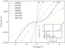
Figure 1 displays the I– V characteristics of Pt/Si/Ta/Ti contact after annealing at different temperatures, measured between the metal pads with a spacing of 10 μ m. The contact properties are dependent on annealing temperature. Like the 4R00, both 4R600 and 4R700 show nonlinear curves, which indicate the Schottky electrical behaviors. The difference is that a sharp decrease in contact resistance is observed for 4R600 and 4R700. After annealing at 800, 900, and 1000 ° C, the I– V curve becomes linear over the whole voltage range, indicating the Ohmic contact property. The contact resistance (Rt) decreases as the annealing temperature is increased. For example, when the spacing between the two metal pads is 20 μ m, the values of Rt are 38.3, 28.4, and 4.3 Ω after the samples have been annealed at 800, 900, and 1000 ° C, respectively. The lowest specific contact resistance (ρ c) is 8.2 × 10− 6 Ω · cm2 for 4R1000 (Table 1). When the temperature is further increased, 4R1050 reverts to Schottky behavior again and the contact resistance is more than that of 4R700. The I– V curve of 4R1100 shows a serious linear deviation and the contact resistance is sharply increased.
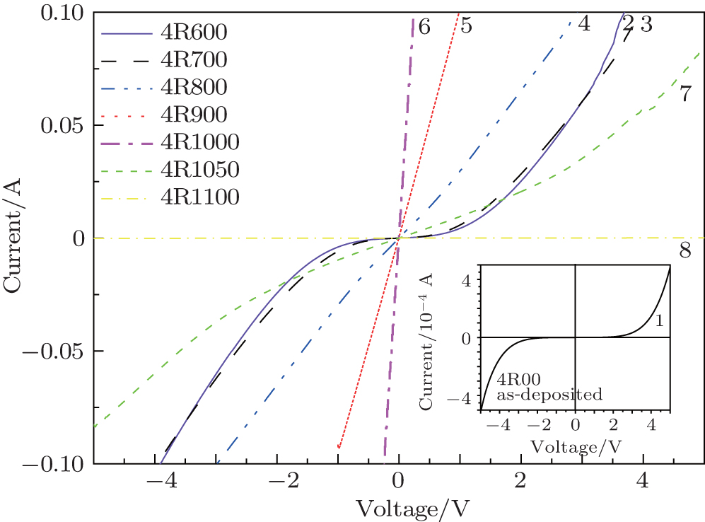 | Fig. 1. Current– voltage characteristics of the Pt/Si/Ta/Ti contacts annealed at different temperatures for 2 min in Ar atmosphere. 1: 4R00; 2: 4R600; 3: 4R700; 4: 4R800; 5: 4R900; 6: 4R1000; 7: 4R1050; 8: 4R1100. |
| Table 1. Summary of the values of specific contact resistance ρ c (Ω · cm2) after the annealed contacts have been aged at 600 ° C in air for different times. |
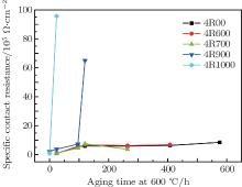
The long-term thermal stabilities of the annealed contacts are electrically evaluated after 24, 96, 120, 264, 408, and 576 h of aging. The values of contact property and ρ c (if the contact was Ohmic) with respect to the aging time are listed in Table 1 and compared in Fig. 2. The 4R1000-24 maintains a good Ohmic contact with the ρ c of 9.57 × 10− 4 Ω · cm2, which is increased by two orders of magnitude in comparison with that of 4R1000. The rectifying behavior appears after the aging time has been prolonged to 48 h. In contrast, the initial rectifying 4R600 becomes Ohmic after it has been aged at 600 ° C for 24 h in air, and the Ohmic property is maintained for up to 408 h. Compared with the initial value of 9.36× 10− 6 Ω · cm2, the ρ c (6.87× 10− 5 Ω · cm2) is only increased one order of magnitude after being aged for 408 h. The performance of 4R00 is similar to that of 4R600. More importantly, 4R00 shows the best long-term thermal stability. Only 4R00 maintains ρ c stable within the experimental error after being aged for up to 576 h. Thus, the Ohmic contact which has been initially unannealed or annealed at 600 ° C appears to be more electrically stable in response to the long-term aging than the 1000-° C annealed Ohmic contacts. The higher annealing temperature is detrimental to the long-term thermal stability of the Ohmic contact.
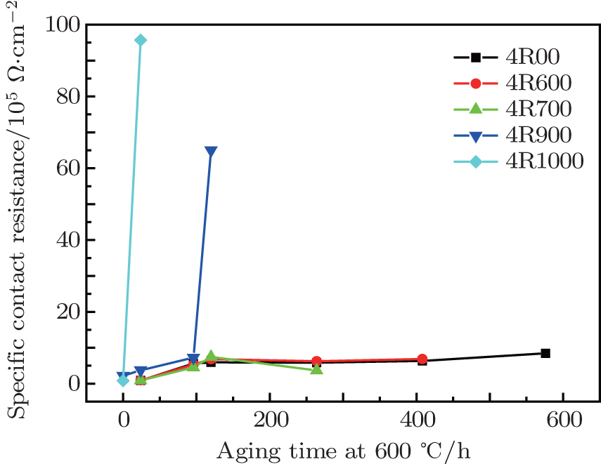 | Fig. 2. Change tendencies of the specific contact resistance after the Ohmic contacts have been aged at 600 ° C in air for different times. |
In order to identify the source(s) of the degradation after being aged, the contacts are characterized by TEM and EDX. Figure 3(a) shows the cross-sectional microstructures of 3R600-24. The 3R600 appears identical to 3R600-24 and, therefore, is not shown here. From the TEM image, the thickness values of Si, Ta, and Ti layers are determined to be about 29.9 nm, 52.4 nm, and 43.3 nm, respectively. The total thickness of the multilayer is 125.6 nm. The inter-diffusion of the two metal layers rarely occurs. The Ti/4H– SiC interface appears structurally abrupt with no evidence of degradation via Ti/4H– SiC interface modification. Nanocracks, or other structural defects associated with potential physical– mechanical contact failure are not exhibited. Figure 3(b) shows the linear mapping element distributions of 3R600-24. The abruptnesses of the Si/Ta/Ti/SiC interfaces indicate little or no reaction at these interfaces, which is in agreement with the TEM cross-sectional characterization.
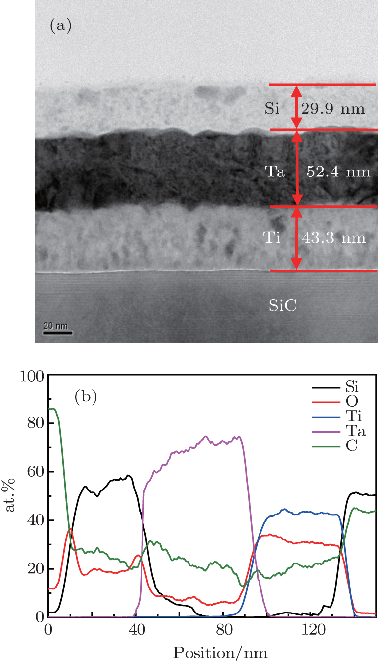 | Fig. 3. (a) Cross-sectional TEM micrograph of the Si/Ta/Ti/4H– SiC contact (3R600-24). The sample is annealed at 600 ° C for 2 min in Ar atmosphere and then aged at 600 ° C for 24 h in air, (b) a linear scanning analysis of the 3R600-24 to display the composition distribution of a selected observation distance. |
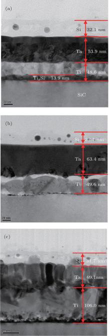
Figure 4 shows comparisons between the cross-sectional TEM images of 3R1000, 3R1000-24, and 3R1100. It is determined that the thickness values of Si, Ta, Ti layers are about 32.1 nm, 53.9 nm, and 48.6 nm, respectively, and the total thickness is 134.6 nm for 3R1000; the corresponding thickness values are 31.0 nm, 64.3 nm, 49.6 nm, and 144.9 nm, respectively, for 3R1000-24. On the one hand, the thickness of 3R600 is smaller than that of 3R1000, suggesting that the contact with SiC interface in 3R600 experiences little or no reaction nor diffusion. In fact, a Ti2.56Si thin layer about 14 nm in thickness is formed at the Ti/SiC interface in 3R1000. Furthermore, compared with 3R1000, the marked increase in contact thickness of 3R1000-24 is indicative of a net movement of the contact material into the SiC substrate and inter-diffusion among metal layers in response to the aging process. The contact experiences elemental diffusion and interfacial reactions, which results in electrical degradation after long-term aging. Thus, even though this contact initially displays the best Ohmic property after being annealed, exposure to prolonged thermal aging at 600 ° C for more than 24 h causes the contact to degrade into rectifying characteristics. The 3R1100 gives an another scenario, in which Ti reacts so seriously with SiC that the thickness of “ Ti layer” is increased to 106 nm. This is the reason why the 3R1100 has a rectifying behavior.
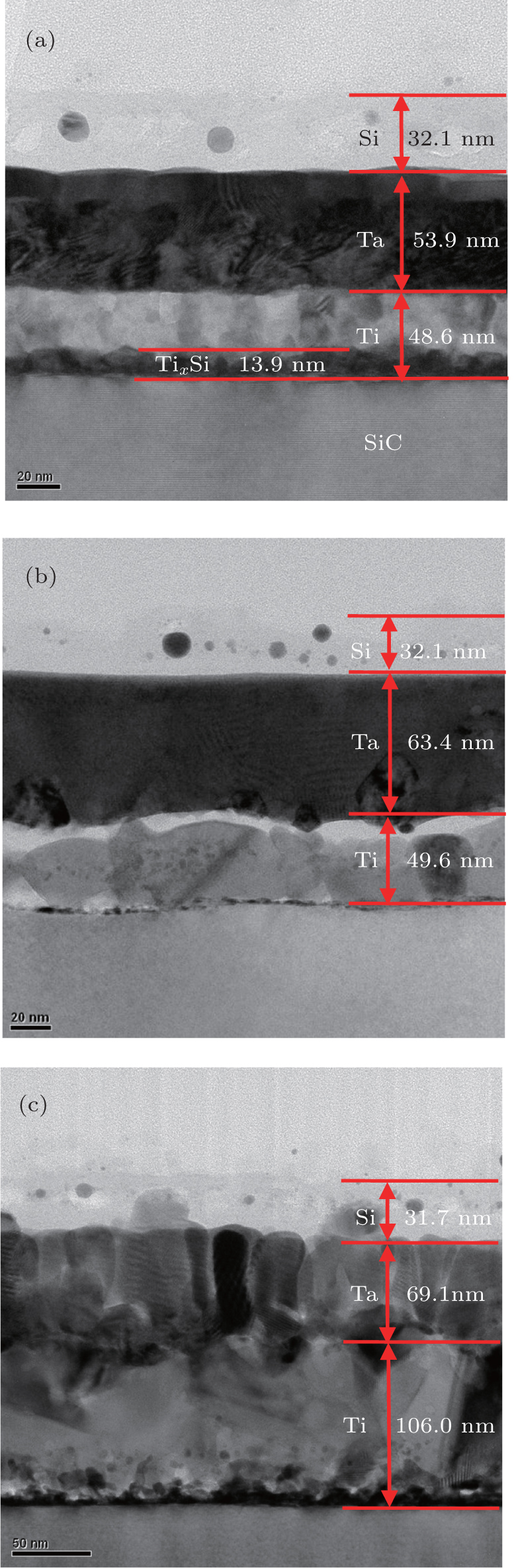 | Fig. 4. Cross-sectional TEM micrographs of the Si/Ta/Ti/4H– SiC contact. (a) 3R1000, (b) 3R1000-24, (c) 3R1100. |
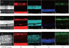
Figure 5 provides further insight into the reaction mechanism through the element distribution mapping. Although the diffusion phenomenon is observed in the interlayer and interface in 3R1000 (Fig. 5(a)), Ta and Ti are still separated from each other and the Ta/Ti interface is sharp. As for the 3R1000-24, the Ta atoms migrate into the Ti layer, which results in the thickness of the Ta layer increasing to 64.3 nm (Fig. 5(b)). In fact, the “ Ta layer” is extended into a Ti layer, and the total thickness of the “ Ta layer” is about 103.9 nm. Few Ti atoms migrate to the Ta layer due to the low diffusivity of titanium. The Si atoms released from SiC substrate migrate upward and those released from the Si layer migrate downward, and the two Si sources meet at the Ta/Si interface. EDX analysis shows that the Ti layer has been completely turned into a roughly 49.6-nm thick inter-diffusion layer with Ta, Ti, and Si elements. The element distributions of 3R1100 and 3R1000-24 resemble each other (Fig. 5(c)). The biggest difference is the ultra-thick (106 nm in thickness) Ti layer in 3R1100. Higher annealing temperature performs two functions, one is to accelerate the reaction between Ti and SiC at the Ti/SiC interface, and the other is to enhance the ability for Ta atoms to diffuse to the Ti layer. It should be mentioned that the interface roughness becomes more obvious as the annealing temperature increases. Figure 5(c) shows that the rough Ti/SiC inter-diffusion layer has a high oxygen concentration. The amount of oxygen atom content sharply increases from 20% (3R600, 3R1000) to 50% (3R1100) in all metal layers. Excess oxidation reaction, which forms TaOy and TiOz (Ti : Ta : O = 4 : 1 : 10) in 3R1100, deteriorates the Ohmic contact so seriously that the contact becomes rectifying.
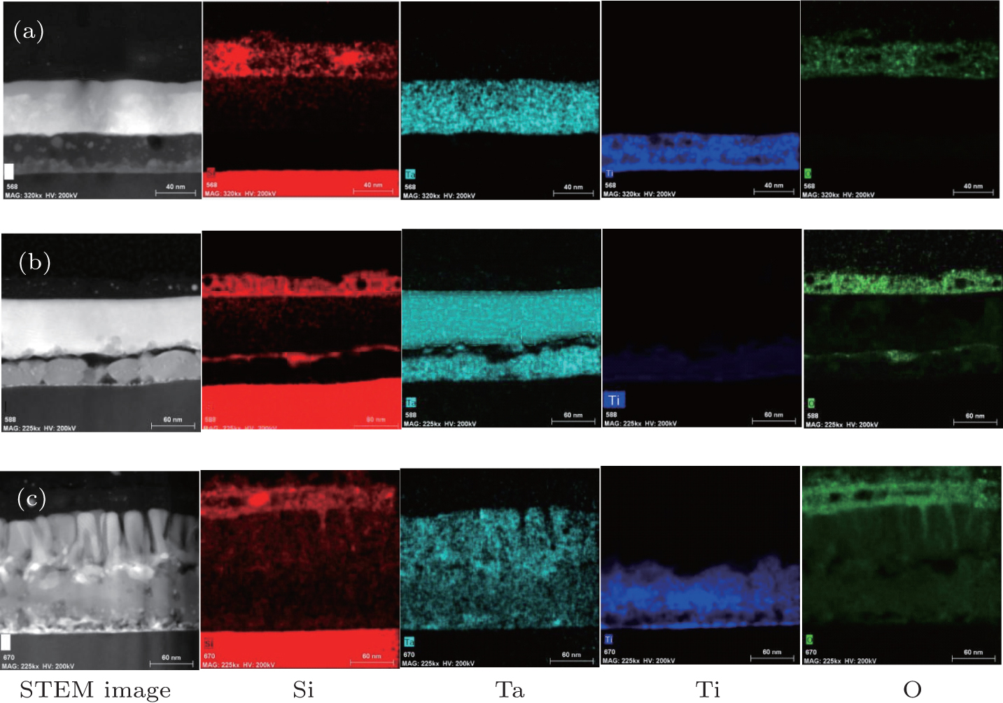 | Fig. 5. Elemental distribution mappings of the Si/Ta/Ti/4H– SiC contacts. (a) 3R1000, (b) 3R1000-24, (c) 3R1100. |
It is accepted that the major contribution to the contact degradation is the interfacial diffusion, the contact/SiC reaction, and the contact oxidation at elevated temperatures for a long-term period.[12, 24] Therefore, the contact reliability for high temperature applications could be better understood within the context of the overall thermo– chemical interactions between the multilayer metallization, the SiC materials, and the outside environment.[14] The experimental results show that the annealing temperature determines the long-term thermal stability of the contact. When the contacts are not annealed, or are annealed at lower temperatures, the long-term thermal stability is satisfactory despite the Shottky behavior in the initial treatment. However, the long-term thermal stability is frustrated when the contacts are annealed at higher temperatures, although the annealed contacts have very low specific contact resistance.
For the annealing temperatures less than 700 ° C, the only chemical and microstructural changes observed are the inter-diffusion of metal atoms at the interface of Si/Ta/Ti/SiC. The aging time is conducive to the formation of an Ohmic contact because the Ti reacts with SiC even at 400 ° C.[25] The stable electrical characteristics for samples annealed at less than 700 ° C imply that the reaction kinetics may be sufficiently slow to allow long-term operation at 600-° C aging temperature treatments.
When the annealing temperatures are more than 800 ° C, the metallurgical reactions (i.e., inter-diffusion, phase transformation, and interfacial roughening) and the oxidation will occur simultaneously, indicating that the metallurgical reactions allows faster oxidation kinetics. One should note that the Ti/SiC interface in 3R1000, which is predicted to be stable and Ohmic, becomes unstable and presents Schottky behavior once additional Ta atoms migrate to the Ti layer in 3R1000-48. Thus, the higher temperature annealed Si/Ta/Ti/SiC contacts are not thermodynamically stable. In addition, the prolonged exposure at elevated temperature during aging allows the contact metallization to continue, resulting in the electrical degradation. Why then are the Ta atoms easier to migrate in the multilayer after the contacts have been annealed at a higher temperature? After careful observation of TEM images of 3R1000 and 3R1100, we find that there is a recrystallization texture or dendritic segregation in the Ta layer. Given that the rapid thermal annealing is similar to the solidification to some extent, it is not surprised for a similar phenomenon to appear, which is widely existent in the alloy solidification. In fact, the aging test at 600 ° C in air is a solute homogeneous process, and the diffusion time (t) is expressed as, [26]

where t is the time when the amplitude of segregation decreases down to 1%, λ the dendrite arm spacing, and D the diffusion coefficient.
The cooling rate in the rapid thermal annealing is dependent on annealing temperature. The higher the annealing temperature, the higher the cooling rate is, which results in the higher density of the dendrites. Therefore, higher annealing temperature makes the dendrite spacing λ smaller. According to Eq. (1), the diffusion time to reach the homogenization (Ta diffusion) is reduced. When the Ta layer becomes loose, its function as an oxygen diffusion barrier partially disappears and the oxygen atoms from the ambient diffuse into the Ti/SiC interface easily. This is the reason why the long-term thermal stability of 3R800 is superior to that of 3R1000 and inferior to that of 3R600 (Fig. 2).
A Ti/Ta/Si/Pt multilayer structure is deposited on n-type 4H– SiC substrate and is then annealed at different temperatures ranging from 600 ° C to 1100 ° C by RTP. An Ohmic contact is formed at 800 ° C and disappears at 1050 ° C. The long-term thermal stability is evaluated by aging the annealed contact at 600 ° C in air. The as-deposited contact property changes from Schottky to Ohmic behavior after being aged for 24 h, showing that the specific contact resistance reaches 9.36× 10− 6 Ω · cm2, and the ρ c of 5× 10− 5 Ω · cm2 is stable for more than 576 h. There is a negative influence on thermal stability with the increase of the annealing temperature. The 1000-° C annealed contact has the lowest specific contact resistance of 8.20× 10− 6 Ω · cm2 and has the shortest life of the thermal stability. The Ohmic contact property deterioration originates from the diffusion of Ta atoms to the Ti layer. Considering the thermal stability, traditional rapid temperature treatment or lower temperature annealing may be worth further research.
| 1 |
|
| 2 |
|
| 3 |
|
| 4 |
|
| 5 |
|
| 6 |
|
| 7 |
|
| 8 |
|
| 9 |
|
| 10 |
|
| 11 |
|
| 12 |
|
| 13 |
|
| 14 |
|
| 15 |
|
| 16 |
|
| 17 |
|
| 18 |
|
| 19 |
|
| 20 |
|
| 21 |
|
| 22 |
|
| 23 |
|
| 24 |
|
| 25 |
|
| 26 |
|