


High response Schottky ultraviolet photodetector formed by PEDOT:PSS transparent electrode contacts to Mg0.1Zn0.9O
[Hu Zuo-Fu, Wu Huai-Hao, Lv Yan-Wu, Zhang Xi-Qing† ]
]
]
|
|


†Corresponding author. E-mail: xqzhang@bjtu.edu.cn
*Project supported by the National Natural Science Foundation of China (Grant No. 50972007), the National Basic Research Program of China (Grant No. 2011CB932703), the National Natural Science Foundation for Distinguished Young Scholars of China (Grant No. 60825407), and the Opened Fund of the State Key Laboratory on Integrated Optoelectronics.
In this paper, we report a Schottky ultraviolet photodetector based on poly (3,4-ethylenedioxy-thiophene) poly(styrenesulfonate) (PEDOT:PSS) transparent electrode contacts to Mg0.1Zn0.9O. The I– V characteristic curves of the device are measured in the dark condition and under the illumination of a 340-nm UV light. The device shows a typical rectifying behavior with a current rectification ratio of 103 at ±2 V, which exhibits a good Schottky behavior. The photo-to-dark current ratio is high, which is 1×10³ at −4 V. A peak response of 0.156 A/W at 340 nm is observed. The device also exhibits a wide response from 250 nm to 340 nm, with a response larger than 0.1 A/W. It covers the UV-B region (280 nm–320 nm), which makes the device very suitable for the detection of UV-B light.
Ultraviolet (UV) photodetectors (PDs) have attracted much attention in recent years due to their wide range of civilian and military applications, such as flame detection and monitoring, bio-agent detection, environmental monitoring, solar astronomy, etc.[1, 2] As a direct wide-bandgap material, MgZnO has been regarded as an excellent candidate for UV detection. MgZnO, which is realized by alloying MgO with ZnO, exhibits the same material advantages as ZnO. Owing to the fact that the ionic radius of Mg2+ is very close to that of Zn2+ , the bandgap of a MgZnO thin film can be changed in a wide range (from 3.37 eV to 7.8 eV) just by adjusting the content ratio of the alloy.[3– 5] The fabrication of a stable p-type MgZnO is still challenging, so the study of a MgZnO Schottky photodetector has been very limited. Among various types of detectors, the Schottky photodetector has many advantages, such as simplicity in fabrication, high quantum efficiency, high response speed, low dark current, high UV/visible contrast, etc.[1] As is well known, the Schottky junction works based on the barrier between a metal and semiconductor when they are in contact with each other. The metals with large work function such as Pt (ϕ = 5.65 eV), Au (ϕ = 5.1 eV), Ag (ϕ = 5.12 eV), and Pd (ϕ = 4.26 eV) have been used as Schottky contacts to ZnO. However, these junction properties are highly dependent on the deposition methods of metals and the surface treatment condition.[6– 9] In recent years, Nakano et al. reported a ZnO-based UV photodiode by using a poly (3, 4-ethylenedioxy-thiophene) poly(styrenesulfonate) (PEDOT:PSS, PH500) transparent Schottky contact.[10, 11] The device showed a good Schottky behavior and high performance in the UV region. The PH500 is widely used as a polymer anode for flexible polymer solar cells.[12, 13] The recent commercial substitution for PH500 is PH1000, which has a higher conductivity than PH500. Because PEDOT:PSS thin film has an internal transmittance of nearly 100% in a wide wavelength range from 250 nm to 800 nm, a resistivity of as low as 10− 3 Ω and a large work function of 5.0 eV, [10, 14– 17] we think that this polymer can also be used as the transparent Schottky contacts to MgZnO.
In this paper, we fabricate a MgZnO/PEDOT:PSS (PH1000) Schottky junction for ultraviolet detection. The current– voltage characteristics and photo-response properties are discussed.
The PD was fabricated on a cleaned quartz substrate, which had been cleaned by ultrasonic bath in ethanol, acetone, and deionized water. Al used as contact electrode was evaporated through a pattern mask on the surface of the quartz substrate. PEDOT:PSS solution (CLEVIOS PH1000, 5% dimethylsulfoxide was added to enhance the conductivity) was spin-coated onto the substrate, and then dried in a vacuum oven at 150 ° C for 20 min. Afterwards, the substrate was loaded in the growth chamber of MBE with a base pressure of 1× 10− 7 Pa. The MBE system equipped with Knudsen-cells for Zn solid source (7 N) and Mg solid source (5 N), and O2 (5 N) was used as an O source activated by Oxford Applied Research Model HD 25 radio frequency (13.56 MHz) atomic source. The Mg component of the MgZnO film was controlled by the temperatures of Mg and Zn sources. A 200-nm thick Mg0.1Zn0.9O film was grown on the substrate, the temperature of the substrate was 100 ° C. After the growth in MBE, a 120-nm thick circular Al electrode with 1-mm diameter was patterned onto the Mg0.1Zn0.9O layer by thermal evaporation through a shadow mask. All of the materials used in this paper were commercially available. The detailed structure of the PD is Quartz/Al contact electrode/PEDOT:PSS transparent electrode (100 nm)/Mg0.1Zn0.9O (200 nm)/Al electrode (120 nm), which is shown in Fig. 1.
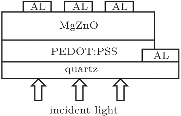 | Fig. 1. Detailed structure of the device. |
The thickness of the film was measured by using an Ambios Technology XP-2 Stylus Profiler. The absorption spectra and transmission spectra were measured by a Shimadzu UV-3101 PC spectrophotometer. The I– V characteristics and photocurrent response of the PD were measured and recorded by a Keithely2410 and a monochromator coupled with a xenon lamp. All of the measurements were carried out in ambient atmosphere at room temperature.
Figure 2 shows the absorption spectra of the Mg0.1Zn0.9O (200 nm) thin film on quartz and the transmission spectra of PEDOT:PSS (100 nm) on quartz. As shown in Fig. 2, it can be seen that the absorption of Mg0.1Zn0.9O film has a high absorption peak at 340 nm and a sharp absorption edge at 360 nm. This indicates that the crystalline quality of MgZnO film is expected. It also means that the MgZnO film used in this PD is suitable for ultraviolet detection. From the transmission spectra of PEDOT:PSS, we could find that the transmittance of PEDOT:PSS film stays constant ∼ 90% from 280 nm to 500 nm, while it sharply drops from ∼ 80% to ∼ 5% in the region from 250 nm to 200 nm. This shows the possibility of using PEDOT :PSS as the transparent electrode.
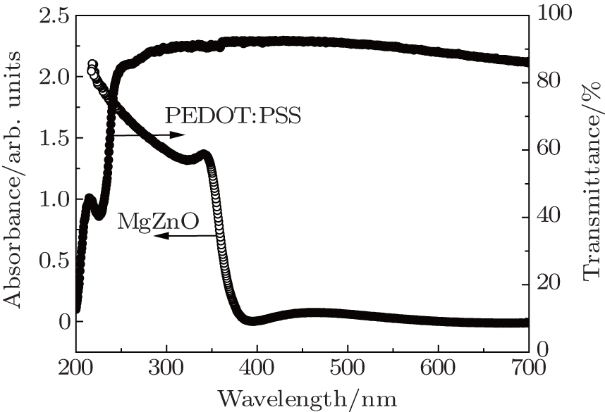 | Fig. 2. Absorption spectra of MgZnO film on quartz and the transmission spectra of PEDOT:PSS film on a quartz substrate. |
The I– V characteristic curves of the PDs, measured both in the dark condition and under the illumination of 340-nm UV light through the quartz side are shown in Fig. 3. The device shows a typical rectifying behavior with a current rectification ratio of 103 at ± 2 V, which exhibits a good Schottky behavior. Moreover, the dark current is very low, which is about 2.3× 10− 8 A at − 4 V. For the high performance of PD, the dark current of the device must be low. High resistivity of the undoped MgZnO film used in this PD is the reason for the low dark-current. As shown in Fig. 3, the photo-current density increases quickly at backward bias. The photo-to-dark current ratio is 1× 10³ at a bias of − 4 V. This means that the PD has high sensitivity and it can detect even a weak UV light in a strong noise background.
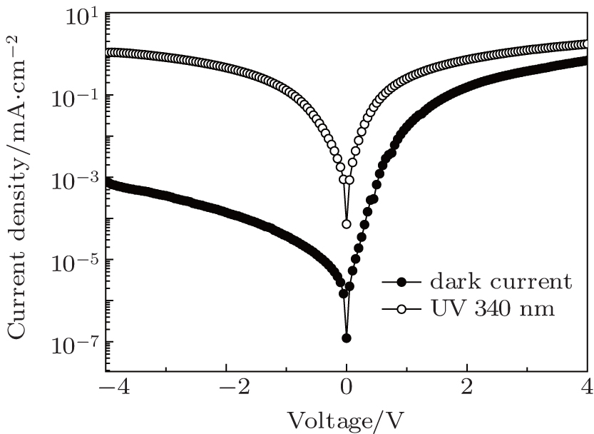 | Fig. 3. I– V characteristics of the device both in the dark condition and under illumination of 340-nm UV light. |
In order to examine the Schottky junction, the I– V curves can be fitted to the general diode equation (1) on the basis of thermionic theory and the barrier height of the junction, ϕ b, can be estimated from the following formula:[18]


where Is is the saturation current, q is the electron charge, V is the applied voltage, n is the ideality factor, A is the junction area, A* is the effective Richardson constant (∼ 32 A· cm− 2· K− 2), and ϕ b is the Schottky barrier height. The values of n = 1.5 and ϕ b = 0.72 eV are obtained from curve fitting.
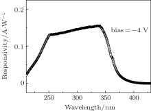
Figure 4 shows the spectrum response of the PD at − 4 V. A peak response of 0.156 A/W at 340 nm is observed. This is comparable to the highest value ever reported in this field. This PD was fabricated based on MgZnO with a Au electrode.[19] Compared with the former one, the PD with PEDOT:PSS electrode is low-cost. Moreover, the device exhibits a wide response from 250 nm to 340 nm, with a response larger than 0.1 A/W. This covers the UV-B region (280 nm– 320 nm). Since the exposure to UV-B light is the main cause of skin cancer, the PD, which can detect the UV-B light, is very useful. The cut-off wavelength of the response is at 380 nm, corresponding with the absorption of MgZnO, this is because the response originates from the MgZnO layer. At a shorter wavelength than 250 nm, the response decreases quickly, which is due to the transmission of PEDOT:PSS. Under 4-V backward bias voltage, the UV (R340 nm)/visible (R400 nm) rejection ratio of the device is two orders of magnitude, which indicates that the device has a high spectral selectivity.
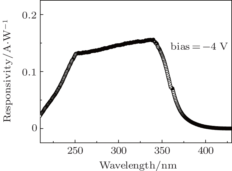 | Fig. 4. Photocurrent response spectrum of the device operated at bias of − 4 V. |
In this work, a MgZnO/PEDOT:PSS Schottky junction is fabricated based on PEDOT:PSS contacts to MgZnO. The current– voltage (I– V) characteristics of the fabricated Schottky junction exhibits a typical rectifying behavior. The PD has a high photo-to-dark current ratio which is 1× 10³. A high response of 0.156 A/W at 340 nm is observed at a bias of − 4 V. We believe that this system can be a promising alternative and can be used to fabricate low-cost and high performance Schottky junctions for UV detection.
| 1 |
|
| 2 |
|
| 3 |
|
| 4 |
|
| 5 |
|
| 6 |
|
| 7 |
|
| 8 |
|
| 9 |
|
| 10 |
|
| 11 |
|
| 12 |
|
| 13 |
|
| 14 |
|
| 15 |
|
| 16 |
|
| 17 |
|
| 18 |
|
| 19 |
|