

Influences of Pr and Ta doping concentration on the characteristic features of FTO thin film deposited by spray pyrolysis
[Turgut Güven†a)  , Koçyiğit Adem‡
b) , Sönmez Erdalc) ]
, Koçyiğit Adem‡, Sönmez Erdal|
|


†E-mail: guventrgt@gmail.com
‡Corresponding author. E-mail: adem.kocyigit@igdir.edu.tr
The Pr and Ta separately doped FTO (10 at.% F incorporated SnO2) films are fabricated via spray pyrolysis. The microstructural, topographic, optical, and electrical features of fluorine-doped TO (FTO) films are investigated as functions of Pr and Ta dopant concentrations. The x-ray diffraction (XRD) measurements reveal that all deposited films show polycrystalline tin oxide crystal property. FTO film has (200) preferential orientation, but this orientation changes to (211) direction with Pr and Ta doping ratio increasing. Atomic force microscopy (AFM) and scanning electron microscopy (SEM) analyses show that all films have uniform and homogenous nanoparticle distributions. Furthermore, morphologies of the films depend on the ratio between Pr and Ta dopants. From ultraviolet-visible (UV-Vis) spectrophotometer measurements, it is shown that the transmittance value of FTO film decreases with Pr and Ta doping elements increasing. The band gap value of FTO film increases only at 1 at.% Ta doping level, it drops off with Pr and Ta doping ratio increasing at other doped FTO films. The electrical measurements indicate that the sheet resistance value of FTO film initially decreases with Pr and Ta doping ratio decreasing and then it increases with Pr and Ta doping ratio increasing. The highest value of figure of merit is obtained for 1 at.% Ta- and Pr-doped FTO film. These results suggest that Pr- and Ta-doped FTO films may be appealing candidates for TCO applications.
The degenerate oxide semiconductors have received great attention. They have been utilized on a large scale as transparent conductive oxide (TCO) electrodes in light emitting diodes (LEDs), solar cells, display devices.[1– 3] Among the TCOs, tin oxide (TO-SnO2) is an n-type wide-band-gap material resulting from oxygen vacancies and tin interstitials.[4, 5] A variety of studies have been carried out about thin film TO because of its convenient electrical and optical features.[6– 9] In order to improve and control characteristic features of TO films, tin oxide can be doped with foreign elements such as F, Sb, Mo, Nb, Nd, Pr, Ta, W, and In. Of them, fluorine is the most important dopant element, because fluorine has caused a very important healing in electrical and optical features of tin oxide. The fluorine-doped TO (FTO) has a commercial importance now, [10] but more studies should be made on FTO films to heal its properties. The praseodymium and tantalum can exist in mixed valance states up to 5+ . The replacement of Sn4+ ions by Pr5+ and Ta5+ ions or substituting any ion states of Pr and Ta in the F-doped SnO2 lattice can lead to an improvement in electrical and optical features of FTO films. In the literature, there has been no study on Pr and Ta separately doped FTO films. Therefore, it is essential to make a study on the Pr and Ta contribution influence on features of FTO so that transparent conductor FTO can be more efficient.
FTO, Pr and Ta separately doped FTO thin films can be prepared by several deposition methods, such as thermal evaporation, [11] sputtering, [12] chemical vapor deposition, [13] spray pyrolysis, [14] reactive evaporation, [15] and the sol– gel spin coating technique.[16] Among these deposition techniques, spray pyrolysis is a useful technique to fabricate thin films due to its basic and cheap apparatus, [17] easy adding of contribution atoms, re-growth capability.[18]
Herein, in this investigation, FTO material is doped with Pr and Ta by spray pyrolysis to change electrical and optical characteristics of FTO. The deposited films are characterized by x-ray diffraction (XRD), atomic force microscopy (AFM), scanning electron microscopy (SEM), Ultroviolet visible (UV-Vis) spectrophotometer and electrical measurements.
Single F, double Pr + F and Ta + F incorporated SnO2 samples were deposited via a spray pyrolysis. The 0.7-M SnCl2· 2H2O dissolved in methanol was used as SnO2 starting solution. For F, Pr, and Ta doping, NH4F, PrCl3· H2O, and TaCl5 were separately solved in ultra-pure water and ethanol solvents, respectively. These solutions were mixed in essential quantities to make 10 wt.% F + 0– 4 at.% Pr incorporated and 10 wt.% F + 0– 4 at.% Ta incorporated solutions. The prepared solutions were pulverized on the glass substrates at 500 (± 5) ° C. The substrates were cleaned with various alcohol and pure water. The other spray parameters like nozzle-substrate distance, flow rate of air, quantity of solutions were fixed to be 40 cm, 3 ml/min, 30 ml, respectively. The 10-wt.% F-doped SnO2, 1-at.% Pr, 2-at.% Pr, 3-at.% Pr, 4-at.% Pr, 1-at.% Ta, 2-at.% Ta, 3-at.% Ta, and 4-at.% Ta-doped SnO2:F films were named FTO, PFTO-1, PFTO-2, PFTO-3, PFTO-4, TFTO-1, TFTO-2, TFTO-3, and TFTO-4, respectively.
The micro-structural characterizations of films were done by a Rigaku/Smart Lab x-ray diffraction (XRD) with CuKα radiation (λ = 0.154059 nm) operated at 40 kV and 30 mA at the room temperature. The XRD data were taken in geometry of coupled θ – 2θ varying between 20° and 80° . The topographic characterization was made by an atomic force microscopy (AFM, which was produced in Nanomagnetics Instrument) and scanning electron microscopy (SEM, inspect FEI 50). The sheet resistance analysis was done with a four-point probe. The optical features were investigated with transmittance analysis taken by UV– Vis spectrometer (Perkin-Elmer, Lambda 35).
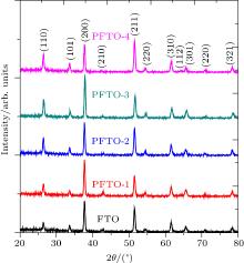
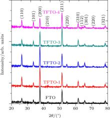
The crystalline structures of PFTO and TFTO films are examined by XRD analysis. The SnO2 tetragonal cassiterite structures (JCPDS 41-1445) are observed from XRD graphs given in Figs. 1 and 2 for PFTO and TFTO films, respectively. The secondary structure peaks, such as SnO, Sn2O3, SnF2, and metallic Pr or Ta compounds have not been identified in the graphs. It could be concluded that doping elements are dispersed homogenously in SnO2 lattice.[14]
As seen from XRD patterns, FTO film has (200) preferential orientation and this orientation changes to (211) plane for high Pr and Ta doping level content. Preferred orientation is very important for determining crystal tendencies in XRD graphs. There are many different causes responsible for preferred orientations in a plane. Some of them are precursor solution chemistry, [19, 20] incorporation of Sn in the SnO2 structure, [21, 22] spray precursor solution molarity, [23] and substrate temperature of sprayed SnO2.[24] In this work, it is shown that the chemical composition of solutions influences the preferential orientations of the films. These kinds of results have been observed by Li et al.[25] for Pr doping and Lee et al.[6] for Ta doping.
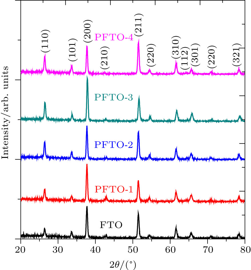 | Fig. 1. XRD patterns of PFTO. |
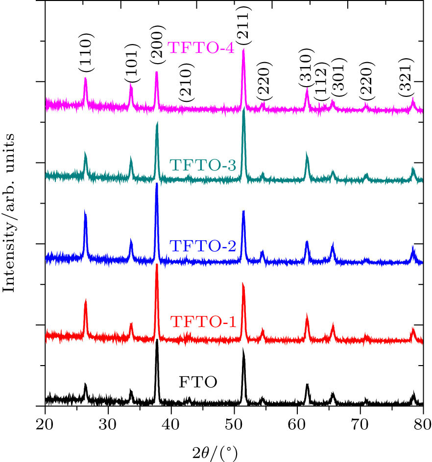 | Fig. 2. XRD patterns of TFTO. |
In PFTO films, peak intensities increase with Pr doping ratio increasing. The 1-at.% and 3-at.% Pr-doped FTO samples have higher intensities than 2-at.% and 4-at.% doped films. In TFTO films, peak intensities also increase with Ta doping level increasing and reach a maximum intensity for 2-at.% Ta doping then decrease with Ta content increasing. The peak intensity of each peak gives information about the growth of polycrystalline thin films. To obtain information about growth mechanism, the texture coefficient (TC) is calculated from the following relation:[26]

where Ihkl, I0(hkl), and N are the observed peak intensity, peak intensity in JCPDS card no: 41-1445, and the reflection number, respectively. The changes of TC with Pr and Ta doping ratio are tabulated in Table 1. If a crystal grain is randomly directed, its TC(hkl) value is equal to one, but the value of TC(hkl) higher than one indicates that the greater quantity of crystallites directed at the (hkl) orientation.[26] In this study, for Pr-doped thin films, the values of TC for (210), (200), and (301) directions are all greater than one for all samples.
| Table 1. TC values of Pr- and Ta-doped FTO samples for different planes. |
FTO film has the highest TC value of (210) and this highest TC value does not change for all Pr-doped FTO films. As FTO is incorporated with 1-at.% Pr, the TC value of (210) peak reaches a maximum value and TC values of (200) and (301) start to decrease. For 2-at.% Pr doping level, TC value of (210) direction decreases and the values for other two peaks increase. After this doping level, TC values of (210) and (301) stay nearly constant but TC value of (200) peak reaches a maximum value for 4-at.% Pr doping level. Moreover, TC value of (321) peak increases up to unity for 3-at.% Pr doping content. All changes for TC values confirm the reorientations in the PFTO films.
TC values of (210), (200), and (301) peaks are higher than unity in all samples for Ta-doped FTO, too. The highest TC values of (210) of FTO film do not change for all Ta-doped FTO films. For FTO, as contribution level is 1-at.% Ta, TC values of (210) and (200) peaks decrease but TC value of (301) stays constant. When contribution level increases until 3-at.% Ta, TC of (210) continues to decrease. However, TC value of (200) continues to increase and TC value of (301) remains constant. For 4-at.% Ta doping, TC quantities of (210) and (301) increase and TC value of (200) decreases. Furthermore, TC value of (321) peak increases up to one with 1-at.% Ta doping content. These changes verify that all TFTO films have reorientations in their structures. This kind of result could be found in Refs. [23] and [27].
Interplanar distance (d) values of the PFTO and TFTO films are calculated by Bragg’ s law:[28]

In this equation, n is a constant generally equal to one, λ is the wavelength of x-ray, and θ is the diffraction angle. Interplanar distances given in Table 2 are nearly the same as the standard d values cited from JCPDS card No:41-1445.
The lattice constants of ‘ a = b’ and ‘ c’ of the tetragonal structure are identified by using the following formula:[29]

where h, k, and l are Miller indices. The determined a and c values in Table 3 agree with those from JCPDS card No.: 41-1445 (a = b = 0.47382 nm, c = 0.31871 nm). Lattice parameters of doped films are higher than the standard lattice values for all doped films, but these parameters do not change with doping contents increasing. The increase in the lattice parameter of the film indicates that F, Pr, and Ta elements penetrate into tin oxide lattice and this case was also observed in earlier studies.[25, 26, 30]
The average crystallite size is evaluated for the most striking peaks with Scherrer relation:[31]

In Eq. (4), D is the crystallite size of nanoparticles, β is the full width at half maximum (FWHM), and θ is the Bragg’ s angle. The values of D have also been given in Table 3 and these values generally increase with Pr and Ta doping level. According to Table 3, D values are 24.27 nm, 25.18 nm, 25.62 nm, 24.54 nm, and 48.90 nm for FTO, PFTO-1, PFTO-2, PFTO-3, and PFTO-4, respectively. For TFTO films, these values are 24.31 nm, 25.55 nm, 27.84 nm, and 28.81 nm for TFTO-1, TFTO-2, TFTO-3, and TFTO-4, respectively. The crystallite sizes of Pr- and Ta-doped films are all bigger than that of undoped FTO. The increasing of crystallite size can be attributed to the replacement of Sn4+ ions with Pr and Ta ions. Such replacements lead to the increases of the crystallite sizes in PFTO and TFTO thin films.[17] The crystalline size variations demonstrate that the Pr and Ta ions have been doped successfully into SnO2 lattice and Pr and Ta dopants have an effect on the increment in the crystalline size.[25]
The geometric mismatchc between film and substrate can cause stress in film[32] and it has a negative effect on structural feature of material. The dislocation and micro-strain (ɛ ) can result from stresses. The values of dislocation density (δ ) and micro-strain for sample are determined from the following expressions:[32, 33]


Dislocation density value of PFTO film does not so change till 4-at.% Pr doping into FTO, and for 4-at.% Pr doping content, dislocation density value decreases sharply which can be attributed to the reorientation of stabler crystal structure.[27] Dislocation density value of TFTO film decreases slightly with increasing Ta doping content. The explanation to this case can also be based on the reorientation of crystal structure. Micro-strain value of FTO film exhibits a decreasing tendency from the value of 10.37 × 10− 4 to the value of 9.83 × 10− 4 in the case of 2-at.% Pr content. Then it increases up to a value of 10.24 × 10 − 4 for 3-at.% Pr, after it decreases sharply to 4.03 × 10 − 4 with 4-at.% Pr dopant. For TFTO samples, micro-strain values continuously decrease from 10.36 × 10− 4 to 6.8 × 10− 4 with increasing Ta doping level. These reductions also attributed to the fact that Pr and Ta elements penetrate into SnO2 lattice.[25]
| Table 2. Calculated and standard d values of Pr- and Ta-doped FTO samples for different planes. |
| Table 3. Some parameters of Pr- and Ta-doped FTO films for preferred orientations. |
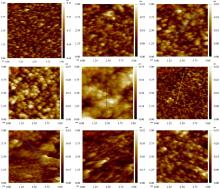
The effects of Pr and Ta doping on morphological structure of spray deposited FTO thin film are investigated by AFM analysis.
The two-dimensional (2D) AFM images of Pr- and Ta-doped FTO films are given in Fig. 3. When AFM images are analyzed in terms of granule gratitude, it is clearly seen that the smallest granule size is in FTO film, whereas the highest granule size is observed from PFTO-1 film. However, it is the evidence that the surfaces of all the samples in the series are granulized and the morphological structures are homogenous. Ta-doped film has bigger grain sizes than FTO film. In the Ta-doped films, surfaces of all the samples are granulized and the morphological structures are also homogenous. Granule sizes increase nearly with increasing up to 2-at.% Ta doping level then decrease.
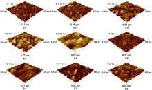
The three-dimensional (3D) AFM images of Pr- and Ta-doped films are shown in Fig. 4. In these films, the smallest granule sizes are observed also in the FTO film. In conclusion, it can be said that Pr and Ta elements have been incorporated into FTO structure.[25]
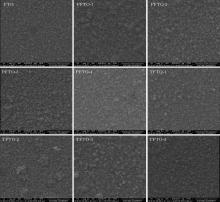
The topographic characterizations for films are also made by SEM images. The SEM images (in Fig. 5 for Pr- and Ta-doped films) indicate that the films are composed of sub-micron particles. These particles are well-defined dense small needle-shaped and pyramidal-shaped. They nearly homogenously dispersed on glass substrate surface. A similar nanoparticle structure was also observed in Ref. [34]. The pyramidal and dense small particles probably belong to (211) and (200) peaks.
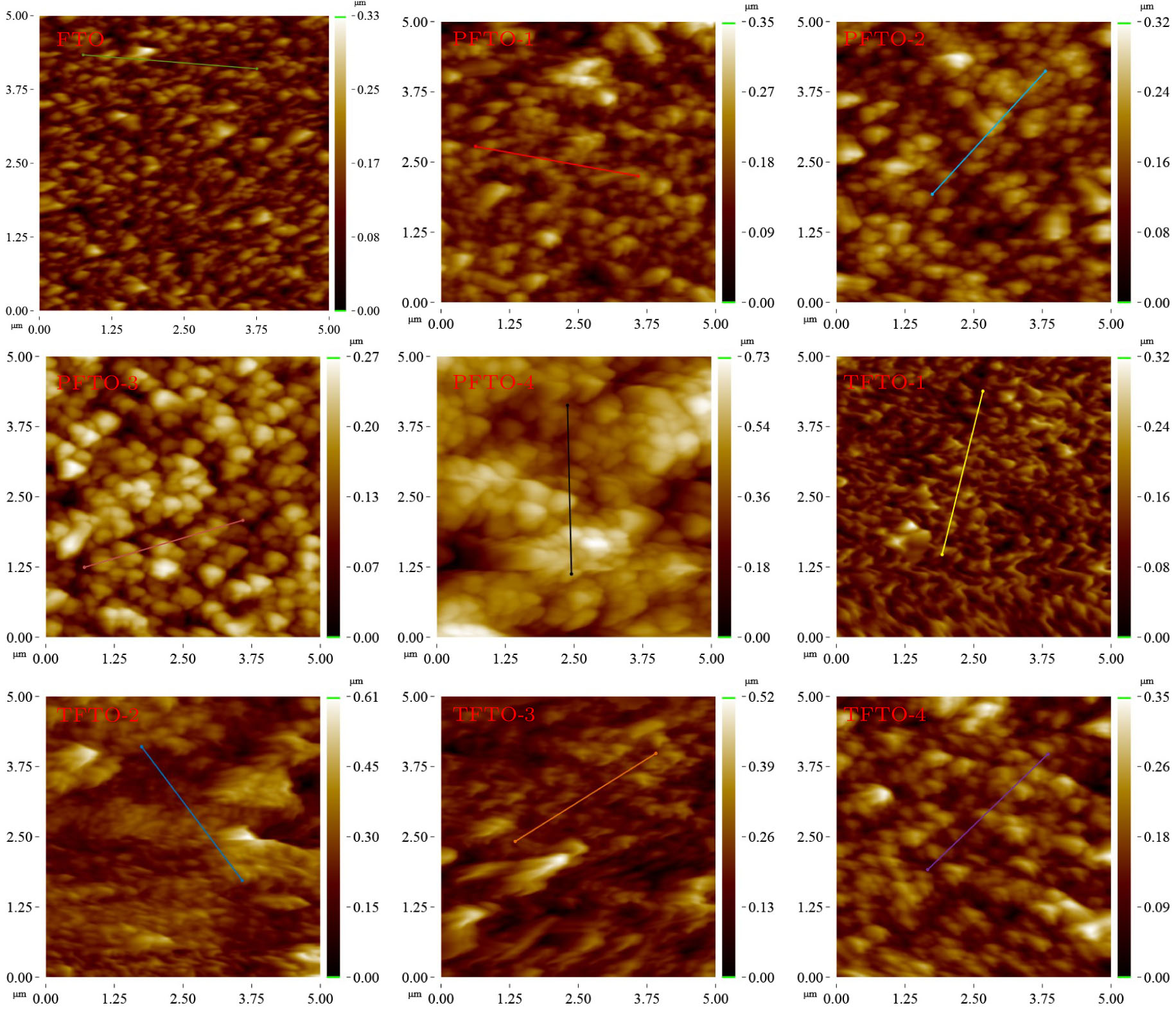 | Fig. 3. The 2D AFM images of Pr- and Ta-doped FTO thin films. |
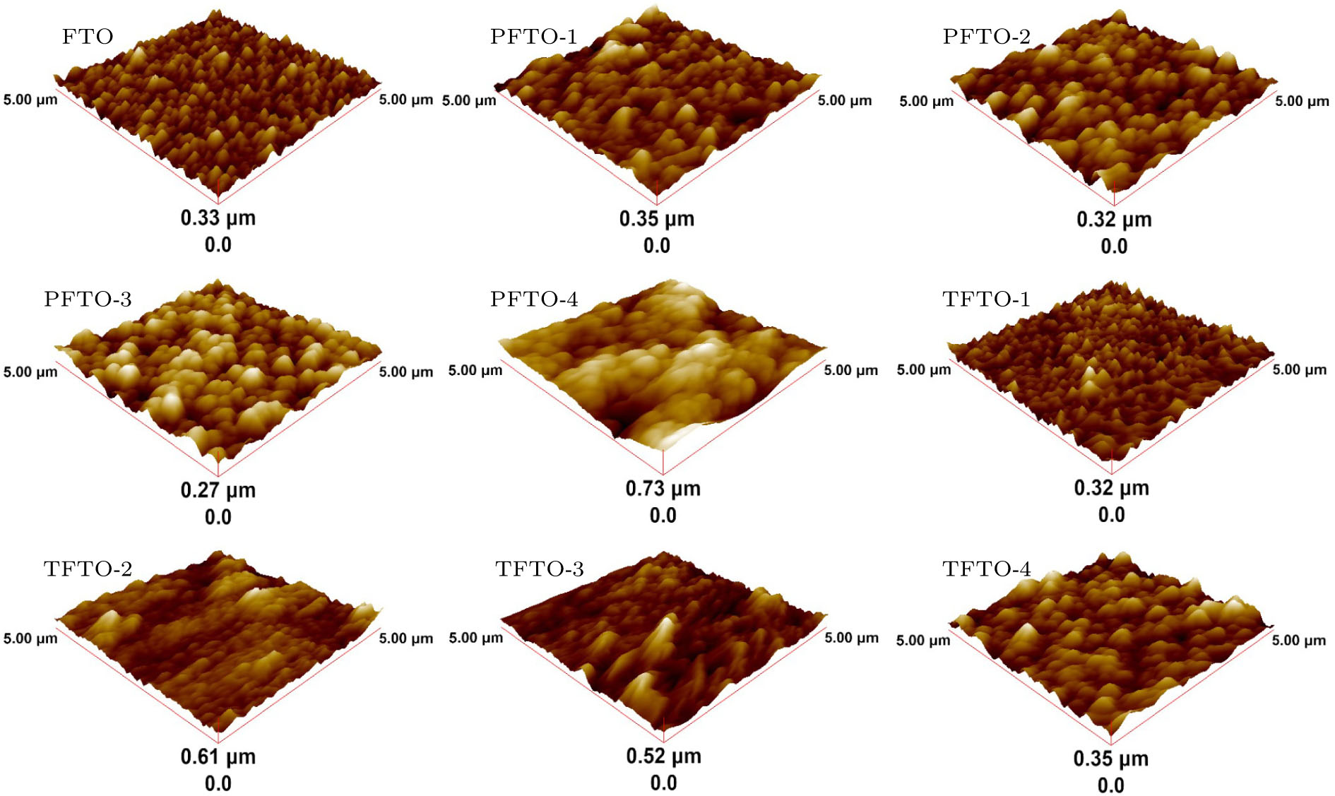 | Fig. 4. The 3D AFM images of Pr- and Ta-doped FTO thin films. |
 | Fig. 5. SEM images of Pr- and Ta-doped FTO films. |
The electrical features of films are investigated with the four-point probe technique. The sheet resistance (Rs) values of the PFTO and TFTO films are shown in Table 4. The sheet resistance of FTO film is 2.51 Ω /□ and it initially decreases to the value of 1.63 Ω /□ in the case of 1-at.% Pr doping. The higher Pr contribution level causes the increase in sheet resistance. For Ta-doped FTO samples, Rs first decreases to the values of 1.70 Ω /□ and 1.27 Ω /□ at 1-at.% and 2-at.% Ta doping levels, respectively, then they increase to the values of 1.96 Ω /□ and 2.29 Ω /□ at 3-at.% and 4-at.% Ta doping levels respectively. The decreasing of sheet resistance can clarify that (i) Pr and Ta elements can exist in various oxidation states up to 5+ [25, 35] and if their 5+ oxidation states are substituted by Sn4+ ions, there will be an increment in free carrier concentration and sheet resistance will decrease; (ii) Pr and Ta ions can be replaced at interstitial lattice positions and they give free electrons to SnO2:F lattice. An increase in sheet resistance of FTO can result from substituting low valance states of Pr and Ta atoms with Sn4+ and structural imperfections.[30] For Ta-doped SnO2, Nakao et al. found that low Ta doping ratio induces the decrease in resistivity of tin oxide and then high Ta content leads to an increase in resistivity.[36] In studies of Sb, [37, 38] F, [22] and doubly doping, [32, 39] it was also found that sheet resistance sharply decreases to nearly one.
| Table 4. Electrical and optical values for samples. |
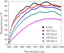
The variations of optical transmittance with wavelength for various PFTO and TFTO films are shown in Figs. 6 and 7, respectively. PFTO films have 60%– 90% transmittance, and TFTO films have 40%– 90% transmittance on the visible region. The FTO film has the highest optical transmittance in all films, and all the optical transmittances decrease with Pr and Ta contribution content increasings.
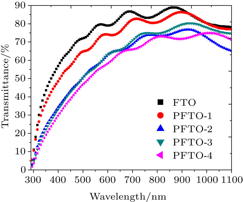 | Fig. 6. Variations of transmittance with wavelength of different PFTO films. |
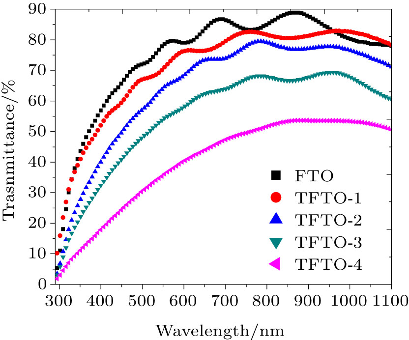 | Fig. 7. Variations of transmittance with wavelength of different TFTO films. |
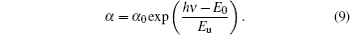
Band gap values of PFTO and TFTO films can be found from transmittance values. The coefficient of absorption (α ) is found from the following equation:[18]

Then (α hν )2 versus hν curves are plotted by using the following equation:[40]

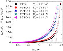
In Eqs. (7) and (8), t is the film thickness, A is a constant, and n = 1. The films prepared in the present study have direct allowed transitions. The curves of (α hν )2 versus hν are plotted in Figs. 8 and 9 for PFTO and TFTO films, respectively. The band gap values for samples are also shown in Table 4. The band gap value of FTO film continuously decreases from 3.92 eV to 3.57 eV with increasing Pr incorporation ratio, however 1-at.% Ta doping gives rise to an increase in optical band gap value of FTO and then it causes continuous decrease in Eg value. The highest band gap value is observed to be 3.98 eV at 1-at.% Ta doping level, another values gradually decrease. This fluctuation could be based on an increase of carrier concentration in the beginning, but a decrease in carrier concentration is responsible for the dropping of band gap values.[41]
This band gap increasing could be expressed as follows; SnO2 is a degenerate semiconductor and its Fermi energy level is inside the conduction band.[42] The band gap of SnO2 is based on the excitation of the electrons from the valance band to Fermi level[7] and an increase in carrier concentration causes Fermi level to increase and optical band gap to broaden. This is known as Moss– Burstein effect.[43] According to the sheet resistance values, it would be expected that 1-at.% Pr and 2-at.% Ta doping cause Eg values of FTO films to increase. But, the re-orientation effect, which can be clearly seen from XRD analysis, could lead to a shift of Eg to lower energy and a red shift of the transmittance.[23]
 | Fig. 8. Band gap energy graphs of PFTO films. |
 | Fig. 9. Band gap energy graphs of TFTO films. |
The localized states around Eg may cause band tails. The absorption edge is known to be the Urbach tail. The energy of Urbach (Eu) is based on possible defects. Eu is given in the following relation:[34]
If logarithm of Eq. (9) is performed, the following equation can be found:
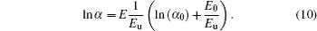
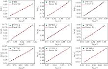
In these equations, E0 and α 0 are constants. The values of Eu for samples are determined from the slopes of ln α versus hν graphs (Fig. 10) by using Eu− 1 = Δ (lnα )/Δ (hν ). The determined Eu values are given in Table 4. The Eu value of FTO film continuously increases from 586 meV to the values of 761 meV, 1231 meV, 1286 meV, and 1360 meV for PFTO-1, PFTO-2, PFTO-3, and PFTO-4, respectively. Similarly, for Ta-doped samples, they increase up to the values of 668 meV, 748 meV, 1320 meV, and 1836 meV for TFTO-1, TFTO-2 TFTO-3, TFTO-4, respectively. The Eu is based on structural defects and an increase in the number of defects causes an increase in Eu.[44] But, for this study, there are discrepancies between structural defects and Urbach energy values. These discrepancies can be attributed to the preferred orientations of the films which are effective to determine dislocation densities and structural defects, and other orientations are also effective to dope an element into the structure, sometimes. The discrepancies of this kind could be seen in Refs. [34] and [45]. The optical band gap values change reversely with Eu values. The broadening of Urbach tail causes the optical band gap of SnO2 to decrease due to transitions from band to tail and from tail to tail.[40]
Steepness parameter (σ st) is temperature-dependent and it characterizes the widening of the absorption edge because of electron– phonon or exciton– phonon interactions.[46] The steepness (σ st) parameter of the film at T = 300 K is calculated from the following equation:

Here, KB is the Boltzmann constant and T is temperature. The steepness value of the sample decreases with adding Pr and Ta dopant into FTO (Table 4). Absorption edge of the film narrows with increasing dopant ratio.[47]
In order to evaluate the efficiency of SnO2 for being utilized as a front contact material, the figure of merit parameter is obtained by Turgut et al.[32] as follows:

The figure of merit values for samples are evaluated to be 550 nm. The determined values are given in Table 4. Figure of merit values of PFTO and TFTO films decrease with increasing doping ratios of Pr and Ta dopants.
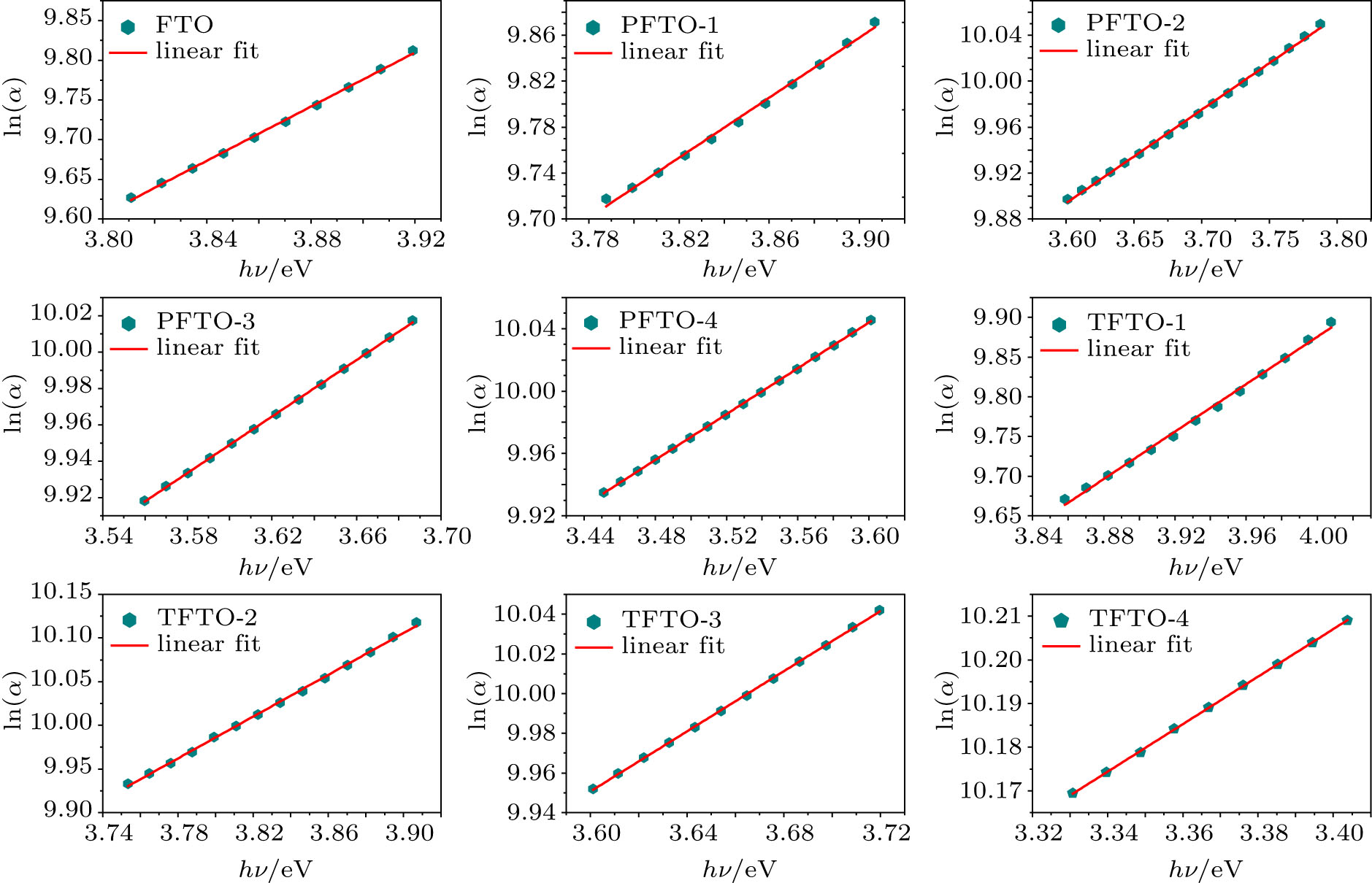 | Fig. 10. Plots of ln(α ) versus hν of PFTO and TFTO films. |
The infrared (IR) reflectivity value of the film is given by relation:[48]

where ɛ 0c0= 1/376 Ω − 1. None of the IR values for FTO, Pr-doped, and Ta-doped FTO films are so changed for different doping ratios (Table 4). All IR reflectivity values are so high for IR reflective coating materials which could be used for heating mirrors.
The PFTO and TFTO thin films are fabricated on glass substrates via spray pyrolysis. The XRD measurements indicate that all films are polycrystalline in nature with tetragonal structure. The AFM and SEM images show that all films are uniform and homogenous. The transmittance values of FTO film decrease with Pr and Ta doping content increasing. Band gap values decrease nearly with increasing the doping ratio for PFTO and TFTO films. The lowest sheet resistance values are obtained for 1-at.% Pr and 2-at.% Ta content. Although the figure-of-merit values continuously decrease with increasing Pr and Ta contribution ratio, IR reflectivity values initially increase at low Pr and Ta level and then it starts to drop off at high contribution content. The results in the present investigation suggest that PFTO and TFTO films can be good candidates for different optoelectronic applications.
| 1 |
|
| 2 |
|
| 3 |
|
| 4 |
|
| 5 |
|
| 6 |
|
| 7 |
|
| 8 |
|
| 9 |
|
| 10 |
|
| 11 |
|
| 12 |
|
| 13 |
|
| 14 |
|
| 15 |
|
| 16 |
|
| 17 |
|
| 18 |
|
| 19 |
|
| 20 |
|
| 21 |
|
| 22 |
|
| 23 |
|
| 24 |
|
| 25 |
|
| 26 |
|
| 27 |
|
| 28 |
|
| 29 |
|
| 30 |
|
| 31 |
|
| 32 |
|
| 33 |
|
| 34 |
|
| 35 |
|
| 36 |
|
| 37 |
|
| 38 |
|
| 39 |
|
| 40 |
|
| 41 |
|
| 42 |
|
| 43 |
|
| 44 |
|
| 45 |
|
| 46 |
|
| 47 |
|
| 48 |
|