Nano LaAlO3 buffer layer-assisted tunneling current in manganite p–n heterojunction
[Ma Jun-Jiea) , Wang Deng-Jing†a), b)  , Huang Hai-Lin
a) , Wang Ru-Wub) , Li Yun-Baoa) ]
, Huang Hai-Lin|
|


†Corresponding author. E-mail: d.j.wang@163.com
*Project supported by the National Natural Science Foundation of China (Grant No. 10804089).
An oxide p–n heterojunction composed of a 150-nm La0.67Ca0.33MnO3 (LCMO) film, 0.05 wt% Nb doped SrTiO3 substrate (STON), and sandwiched 5-nm LaAlO3 (LAO) thin film is fabricated with the pulsed laser deposition technique and the interfacial transport properties are experimentally studied. The rectifying behavior of the junction is in agreement with Newman’s equation, indicating that tunneling is the dominant process for the carriers to pass through the interface while thermal emission is the dominant transport model of an LCMO/STON heterojunction with no LAO buffer layer.
Since Sugiura first fabricated the manganite-based p– i– n heterojunction, [1] p– n heterojunctions based on perovskite manganite oxides have attracted considerable attention[2– 5] because of their potential applications in future electronic devices with multifunctional properties. Compared with the conventional semiconductor junction, and in addition to their excellent rectifying characteristics, manganite-based p– n junctions are expected to exhibit much more powerful functions. In particular, the properties can be tuned by an external magnetic field, such as magnetocapacitance effect, [6] strongly bias-dependent magnetoresistance, [7] and magnetic-field-tunable photovoltaic effects.[8] The previous studies have revealed that thermal emission and tunneling are two main transport processes for the manganite p– n heterojunctions. When the thermal emission is the dominant process for the transport of the heterojunction, an external magnetic field has little effect on the transport properties of the junction. Even the field affects the energy band of the manganite and makes it show a colossal magnetoresistance effect.[9, 10] On the other hand, when the tunneling is determinant for the transport process, the transport properties of the manganite heterojunction can be strongly affected by the external magnetic field.[10, 11] So it is helpful to increase the proportion of tunneling current in the total current from the application point of view. However, because of the existence of a thick depletion layer that is induced by the diffusion of interfacial carriers, it is not easy to obtain the high proportional tunneling current. There have been several successful attempts at increasing this proportion. For example, Xie et al.[12] has reported the tunneling transport process of the heterojunction composed of ultra-thin La0.9Ca0.1MnO3 + δ film and high carrier concentration SrTiO3. Meanwhile, Cuellar et al.[13] have reported the thermally assisted tunneling transport in a heterojunction composed of La0.7Ca0.3MnO3 and low carrier concentration SrTiO3 at low temperature.
In the present paper, we report the transport properties of an La0.67Ca0.33MnO3(LCMO)/LaAlO3(LAO)/0.05-wt% Nb-doped SrTiO3(STON) p– n heterojunction. By analyzing the current– voltage curves at various temperatures, we determine the Schottky-like behavior of the heterojunction and find that tunneling is the dominant process for the heterojunction, while the thermal emission process is dominant for a heterojunction without a LAO buffer layer.
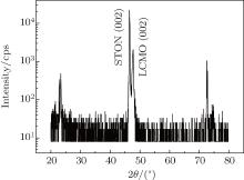
Because of the similarity in lattice constants, the LCMO/LAO/STON heterojunction was fabricated by growing a LAO buffer layer and a LCMO film on the (001) STON substrate by using the pulsed laser deposition technique. First, the LAO layer with a thickness of 5 nm was deposited on a STON substrate, followed by a 150-nm LCMO film. The thickness values are estimated based on the calibrated growth rates of LAO and LCMO films. The substrate temperature was kept at 750 ° C and the oxygen pressure was kept at 1 Pa for LAO and 100 Pa for LCMO during the deposition. The as-deposited sample was cooled to room temperature in the furnace in an oxygen atmosphere with a pressure of 160 Pa, which was done to remove the oxygen vacancies. An LCMO/STON heterojunction without the LAO buffer layer was also fabricated under the same deposition condition for a comparison study. The x-ray diffraction (XRD) data of the LCMO/LAO/STON heterojunction are shown in Fig. 1. Besides the (00l) peaks of the LAO/LCMO film and STON substrate, no others peaks that are observed. This indicates that the LAO/LCMO film is clean single phase and is highly textured.
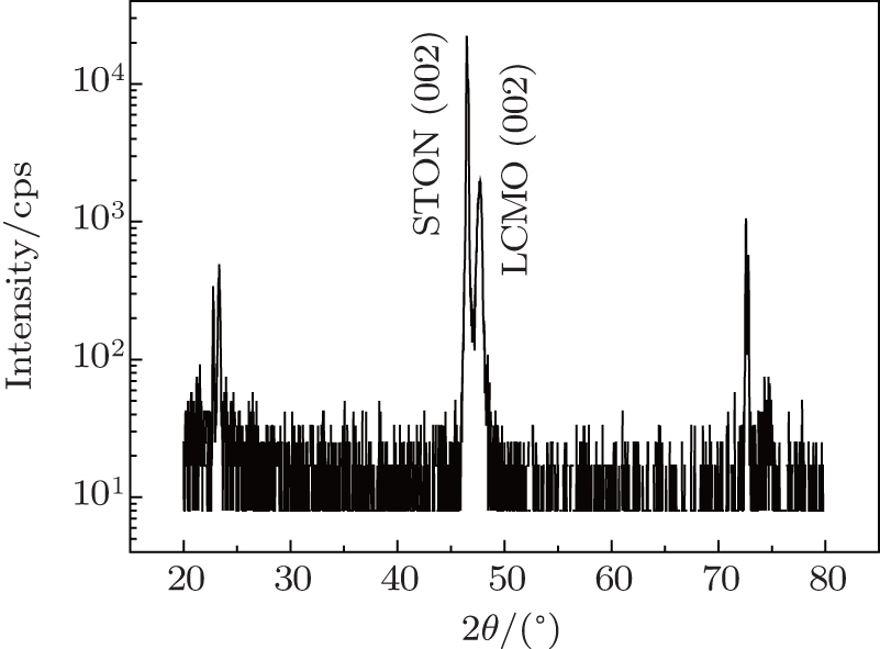 | Fig. 1. The XRD spectra of the LCMO/LAO/STON heterojunction. |
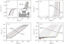
The electrical properties of the heterojunctions were measured by two-point geometry (a schematic diagram of the sample and electrical measurement is shown in the inset in Fig. 2(a)). Three copper electrodes each with a thickness of ∼ 200 nm, two on the STON substrate and the other on the LCMO film, were deposited to avoid the effect of current distribution in the junction[14] and to obtain a good electric contact. The copper electrodes and LCMO film were then patterned into squares, each with a size of 1 mm× 1 mm, by conventional photolithography and the chemical etching technique. The contact resistance of the Cu/STON and Cu/LCMO interfaces, which are both lower than 1 Ω at room temperature, is small enough to ignore. Here, we explain why copper is adopted as an electrode material. The first reason is that the copper is deposited on LCMO and STON conveniently, and it then adheres to LCMO and STON strongly. The contact resistance Cu/LCMO, which is regarded as a metal– metal contact, is small and can be ignored. Usually, the contact resistance between copper and STON is very large because of the existence of the Schottky barrier. A high pulse voltage was applied between the two Cu electrodes on the STON substrate to breakdown the barrier. Finally, the resistance between the two Cu electrodes on the STON is only 1.5 Ω , which indicates that the average Cu/STON contact resistance is lower than 1 Ω and will not affect the quantitative analysis of the transport properties of the junction.
 | Fig. 2. Rectifying characteristics (a) and semilogarithmic plots of the characteristics (c) of a LCMO/LAO/STON junction, and rectifying characteristics (b) and semilogarithmic plots (d) of the characteristics of a LCMO/STON junction, measured at different temperatures from 60 K to 360 K. (The inset of Fig. 2(a) shows the schematic diagram of the sample and electrical measurement.) |
Figure 2(a) shows the current-bias (J– V) characteristics of the LCMO/LAO/STON heterojunction, which are measured at various temperatures by using a superconducting quantum interference device (SQUID) magnetometer equipped with an electrical measurement device. The J– V characteristics of the compared sample LCMO/STON junction are also shown in Fig. 2(b). Both of the junctions exhibit excellent rectifying properties, as shown by the strong nonlinear current dependence of bias and the asymmetry with respect to the direction of the bias. The current is negligibly small and remains tiny in the initial stage of the bias in both directions, but it grows rapidly when the bias voltage exceeds a threshold value of direction dependence. In the forward direction, the threshold is a few tenths of a volt for both the two junctions. In the reverse direction, the threshold is about 1 V for the LCMO/LAO/STON junction. However, for the LCMO/STON junction, the current is still tiny until the bias reaches − 6 V, indicating that the heterojunction has a better anti-breakdown ability than the LCMO/LAO/STON junction. The difference between the rectifying abilities may be ascribed to the difference in transport mechanism between the two heterojunctions, which will be discussed below.
In order to understand the transport mechanism of the junctions, the J– V curves are further analyzed. Figures 2(c) and 2(d) show the semilogarithmic data of the forward direction J– V curves of LCMO/LAO/STON and LCMO/STON junctions, respectively. For both of the junctions, the satisfactory linear relations between log (J) and V are observed in a temperature range from 60 K to 360 K. According to the classical semiconductor theory, [15] the forward current is composed of a thermal current and a nonthermal current. To produce thermal current, charge carriers must overcome the potential barrier to cross the junction region. In this case, temperature plays an important role in activating the charge carriers and the slope of the ln (J)– V curve is expected to be proportional to 1/T. Under such conditions, the thermal current at forward bias is approximately described as

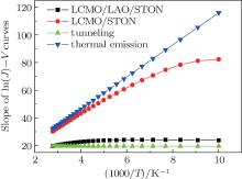
for eV > nkBT. Here, the prefactor J0 is the reverse saturation current, which is related to Schottky barrier, n is the ideality factor (n is expected to be unity for the idealized thermal current), and kB is the Boltzmann constant. The slopes of ln(J)– V curves of the LCMO/STON heterojunction depending on 1/T are shown in Fig. 3. As can be seen, the given relation is in good agreement with the ideal thermal emission model, indicating that thermal emission is the dominant means of a carrier to overcome the interfacial barrier. This result is consistent with the fact that the ideality factor n is pretty small, varying between 1.0 and 1.2 in a temperature range from 130 K to 360 K, which is very close to that (n = 1) of the ideal thermal emission model. However, the experimental results of the LCMO/LAO/STON heterojunction are different from those of LCMO/STON heterojunction. It can be seen in Fig. 2(c) that the log(J)– V curves at various temperatures are almost parallel to each other. Reducing temperature causes the J– V curves to shift downward nearly rigidly. The slope of ln(J)– V is nearly constant and is independent of temperature (Fig. 3), which implies that the electrical transport mechanism of the LCMO/LSO/STON heterojunction is totally different from that of LCMO/STON heterojunction. This is not a thermal emission process but it is a tunneling process, which has been discussed by Newman, and the forward current is described as the Newman equation[16]

where the parameters J0, T0, and E0 are dependent on V weakly.
 | Fig. 3. Slopes of temperature-dependent ln(J)– V curves. The data of the thermal emission and tunneling processes are shown for comparison. |
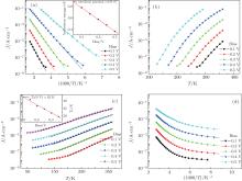
According to Eqs. (1) and (2), for a thermal emission model, the log(J) varied linearly with temperature 1/T if measured under a fixed bias, while it will vary linearly with T for a tunneling model. Figure 4 shows the current dependency on temperature for LCMO/STON and LCMO/LAO/STON heterojunctions, measured under fixed bias voltages of 0.1, 0.2, 0.3, 0.4, and 0.5 V respectively. For the LCMO/STON heterojunction, a satisfactory linear relation between log(J) and 1/T (Fig. 4(a)) and nonlinear relation between log(J) and T (Fig. 4(b)) is observed in a wide temperature range, which is also evidence for the transport properties of the LCMO/STOM heterojunction based on the thermal emission model. The relation between current and temperature can be described as J = J0 exp(− EA/kBT), where parameter EA is the activation energy of the heterojunction under a fixed measuring bias. The values of EA for the present heterojunction under various measuring bias voltages, which are deduced from the slops of log(J)– 1/T curves, are shown in the inset of Fig. 4(a). The linear dependence of activation energy EA on bias is observed. By extrapolating the EA-bias line to zero bias, the interfacial barrier of the junction is obtained to be 0.87 eV, which is similar to the other reported results.[17, 18] A comparison between LCMO/LAO/STON heterojunction and LCMO/STON heterojunction shows that no linear relationship between log(J) and 1/T is observed (Fig. 4(d)). Instead, in a wide temperature region, the linear relationship between log(J) and T (Fig. 4(c)) is observed, which also indicates that the transport properties of the LCMO/LAO/STOM heterojunction are based on the tunneling model.
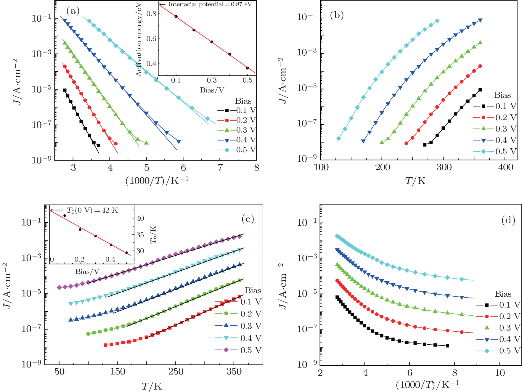 | Fig. 4. Curves of current of LCMO/STON heterojunction versus 1/T (a) and T (b), measured under various biases, the inset in panel (a) shows the line relation between activation energy and bias. The curves of current of LCMO/LAO/STON heterojunction versus T (c) and 1/T (d). The inset of panel (c) shows a linear relation between the parameter T0 and bias. |
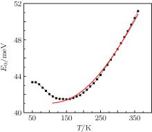
According to Eq. (2), the parameter T0 (the inset of Fig. 4(c)) of the LCMO/LAO/STON heterojunction can be deduced from the curve log(J)– T. T0 increases slowly with the decrease of bias and approximately follows a linear relationship with the bias. The value of T0 under zero bias is obtained to be 42 K by extrapolating the T0-bias line to zero bias. The parameter E0 is also deduced from the log(J)– V curves (Fig. 2(c)) and dependent on temperature as described below[19]

Here, the E00 is a parameter relating to the electron effective mass, donor concentration, and dielectric permittivity of STON. Figure 5 shows the E0 dependence on temperature. E0 is 51 meV at 360 K and it decreases slowly as temperature drops. But it increases with the decrease of temperature below 100 K, which may be ascribed to the nonlinearity of log(J)– V curve at low temperature, which causes the deviation in calculating E0. Above 150 K, the relation between E0 and temperature is in good agreement with Eq. (3), if the value of E00 is assumed to be temperature-independent, with a value fixed at 41 meV.
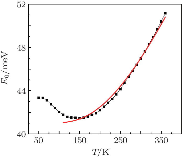 | Fig. 5. E0 dependence of temperature. The thin solid curve is the fitting to Eq. (3). |
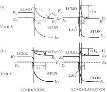
It is obvious that the transport model of the LCMO/STON and LCMO/LAO/STON heterojunctions are not the same as each other, which results from the difference in interfacial energy band structure between the heterojunctions. Schematic diagrams for the energy band structure of heterojunctions are shown in Fig. 6. In the LCMO, three of the Mn-3d electrons form the t2g band, and the remaining electrons occupy the Eg band. The eg band further splits into two sub-bands, eg1 and eg2, with an indirect gap of several tenths of eV due to the Jahn– Teller effect. The eg2 band is completely empty whereas the eg1 band is partly occupied, which forms the conduction and valence bands. The STON is an n-type semiconductor with an energy gap of 3.2 eV. An energy barrier could be formed in the junction region because of the interdiffusion of the holes in LCMO and the electrons in STON. For the LCMO/STON heterojunction, the depletion layer, which is estimated to be 22 nm in thickness, [17] is thick enough to prevent the electrons from tunneling through the energy barrier. However, for the LCMO/LAO/STON heterojunction, the 5-nm LAO buffer layer existing between LCMO film and STON substrate prevents the charge carriers from interdiffusing, forming a thinner depletion layer, which provides a possibility for the electrons to tunnel through the depletion layer of the LCMO/LAO/STON heterojunction easily. On the other hand, although the LMO/LAO/STON heterojunction has a thinner depletion layer, its effective barrier is higher than that of LCMO/STON heterojunction because of the wide band gap (∼ 5 eV) of the LaAlO3 buffer layer.[20]
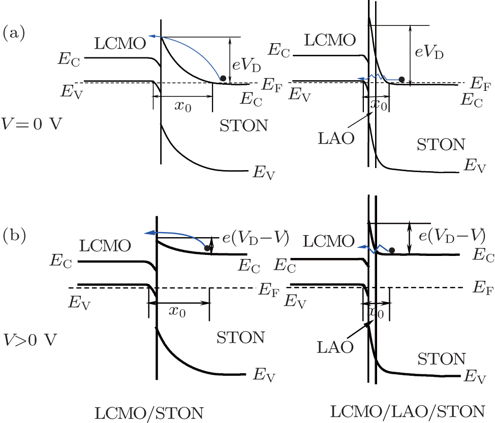 | Fig. 6. The schematic energy band diagrams of LCMO/STON and LCMO/LAO/STON heterojunctions with (a) V = 0 V and (b) V > 0 V. |
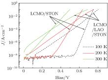
Figure 7 shows the comparisons of J– V curve among LCMO/STON and LCMO/LAO/STON heterojunctions under 100, 200, and 300 K. Under the low bias, the electrons in the LCMO/STON heterojunction have a small possibility to overcome the interfacial barrier by thermal emission, while the electrons in LCMO/LAO/STON heterojunction have a larger possibility to tunnel through the barrier, resulting in the lower current in the LCMO/STON heterojunction and providing the LCMO/STON heterojunction with the ability to be better rectified and anti-broken down. When the bias approaches to the interfacial barrier of the LCMO/STON heterojunction (Figure 6(b) shows the schematic diagrams for the energy band structure under such a condition), the possibility for electrons in LCMO/STON to overcome the barrier increases much more rapidly than that in LCMO/LAO/STON heterojunction, in which the electrons overcome the barrier still by tunneling because of the higher interfacial barrier, consequently the current is larger in the LCMO/STON heterojunction.
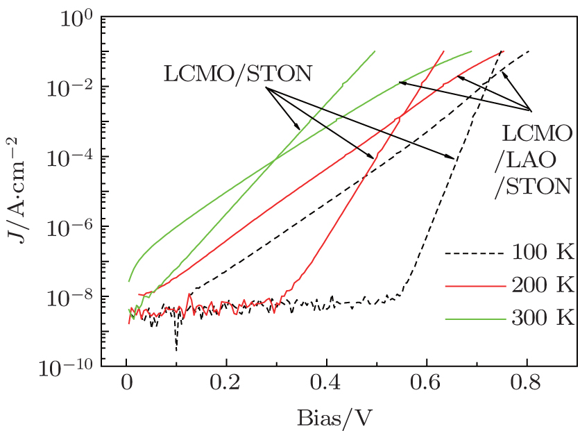 | Fig. 7. Comparisons of J– V curve between LCMO/LAO heterojunction and LAMO/LAO/STON heterojunction under 100, 200, and 300 K. |
The present LCMO film is a typical colossal magnetoresistance effect material with a metal– insulator transition (MIT) at 250 K, and it is expected that the MIT should affect the transport properties of the heterojunctions. However, the results show that the transport properties of both of the heterojunctions have no significant change near the MIT temperature of LCMO. Such phenomena have been reported in a previous work.[17] These results may be ascribed to the existence of the MIT insensitive layer of the manganite and the thick depletion layer of the heterojunction.[9]
A manganite heterojunction LCMO/LAO/STON is fabricated using the PLD technique and the transport properties of the interface are experimentally studied in this work. The rectifying behavior of the junction is well described by the Newman equation. Further analysis shows that transport properties of the heterojunction are based on the tunneling model, while the transport properties of the heterojunction LCMO/STON without LAO buffer layer are based on the thermal emission model. The buffer layer LaAlO3 film in the LCMO/LAO/STON heterojunction plays two kinds of roles. One is the thinner depletion layer and the other is the higher interfacial barrier. The present results demonstrate that the interfacial properties of the manganite heterojunctions can be modified by a nano insulator buffer layer, for a potential manganite application.
| 1 |
|
| 2 |
|
| 3 |
|
| 4 |
|
| 5 |
|
| 6 |
|
| 7 |
|
| 8 |
|
| 9 |
|
| 10 |
|
| 11 |
|
| 12 |
|
| 13 |
|
| 14 |
|
| 15 |
|
| 16 |
|
| 17 |
|
| 18 |
|
| 19 |
|
| 20 |
|