


Mechanical strains in pecvd SiN x:H films for nanophotonic application
[Semenova O.†a)  , Kozelskaya A.
b) , Zhi-Yong Lic) , Yu-De Yuc) ]
, Kozelskaya A.|
|


†Corresponding author. E-mail: oisem@isp.nsc.ru
*Project supported by RFBR (Grant No. 14-03-91154 NNSF) and the National Natural Science Foundation of China (Grant No. 61411130212).
Hydrogenated amorphous silicon nitride films (SiN x:H) are deposited at low temperature by high-frequency plasma-enhanced chemical vapor deposition (HF PECVD). The main effort is to investigate the roles of plasma frequency and plasma power density in determining the film properties particularly in stress. Information about chemical bonds in the films is obtained by Fourier transform infrared spectroscopy (FTIR). The stresses in the SiN x:H film are determined from substrate curvature measurements. It is shown that plasma frequency plays an important role in controlling the stresses in SiN x:H films. For silicon nitride layers grown at plasma frequency 40.68 MHz initial tensile stresses are observed to be in a range of 400 MPa–700 MPa. Measurements of the intrinsic stresses of silicon nitride films show that the stress quantity is sufficient for film applications in strained silicon photonics.
Thin films of hydrogenated silicon nitride fabricated by plasma-enhanced chemical vapor deposition (PECVD) have been widely used in the semiconductor industry as passivation layers, diffusion barriers, gate dielectrics, and also as materials for micro-electro-mechanical systems (MEMS) and antireflection coatings for silicon solar cells.[1– 5] In the past decade the applications of silicon nitride thin films have been extended to silicon photonics.
The influence of strain in the thin films on the properties of devices is a long known effect.[6] The strain appears from different steps in the CMOS (complementary metal– oxide– semiconductor) process and often is a reason for device degradation. This problem becomes even more significant for devices on a nanoscale. However, besides the undesired effects strain can also be used to enhance the desired physical properties of nanostructured devices as already done in the field of strained silicon CMOS technology.[7]
Another field of investigations that is still developing is strained silicon photonics.[8– 10] The goal of silicon photonics is to investigate the integration of individual photonic devices with microelectronic devices that enables high-performance, cost-effective optical communication, and computing systems. The inversion symmetry of silicon crystal prohibits the existence of a linear electro– optic effect. It was shown experimentally and theoretically by Govorkov et al.[11] that the symmetry can be broken by applying inhomogeneous stress in silicon surface layers. Now this idea helps to realize an all-silicon electro– optic modulator based on a strain-induced Pockel’ s effect in silicon. A Mach-Zehnder modulator based on a locally strained waveguide structure is presented in Ref. [12]. The authors used a silicon nitride strain layer deposited directly on the top of the silicon rib-waveguide.
The silicon nitride thin films produced by PECVD tend to be non-stoichiometric and contain hydrogen due to the gas precursors (SiH4 and NH3) used for deposition. Structures and properties of SiNx:H films depend on the deposition rate, substrate temperature, plasma power, pressure in the deposition chamber, gas composition, etc. For applications in photonic devices it is necessary for films to have high intrinsic stresses (above 600 MPa).
Currently, there are only two methods that are described to obtain strain layers of hydrogenated amorphous silicon nitride films. The authors in Ref. [13] presented the measurement results of the intrinsic stresses of silicon nitride films deposited by PECVD with dual plasma excitation frequencies. By changing only the duty cycle of the high (13.56 MHz) and low (380 kHz) plasma excitation frequencies throughout the deposition it was possible to control the stresses of the films, and stress can vary from tensile (up to 500 MPa) to compressive (− 850 MPa). A highly tensile silicon nitride layer is obtained by using cascaded ultraviolet (UV) irradiation in Ref. [14]. Successive UV radiation of equal or shorter wavelengths with variable intensity and duration selectively breaks bonds in the Si– N matrix and minimizes shrinkage and film relaxation. In this case higher tensile stress than a non-cascaded approach may be obtained.
In this work, we investigate the influences of plasma frequency and power on the film properties and particular stresses. The main goal is to develop the process of deposition SiNx:H films with high intrinsic stress.
A parallel-plate PECVD system was used for depositing SiNx:H films. The distance between the electrode and the substrate was fixed at 40 mm and the substrate temperature was equal to 160 ° C or 250 ° C. The films were prepared by using high frequency (HF) plasma (at frequencies of 40.68 MHz and 13.56 MHz respectively). A gas mixture of SiH4 and NH3 was used as precursor. Argon was chosen as diluent gas. The gas flow-rate ratio was fixed (SiH4/NH3 = 1/6), pressure in the reactor changed from 10 Pa to 26 Pa, and power densities dissipated on the electrode ranged from 0.05 W/cm2 to 0.3 W/cm2. As a substrate we used single crystal silicon wafers, single crystal germanium wafers and prisms. We used the standard procedure for chemically treating the substrate surfaces: degreasing in trichloroethylene, boiling in NH3– H2O2 solutions and treatment by hydrogen fluoride (HF). The refractive index and thickness of the layers were estimated by using an LEF 3M laser ellipsometer (632.8-nm laser wavelength). The SiNx:H film thickness was 200 nm. Distribution of the film thickness along the Si substrate was measured by using a “ MICROSCAN-M” scanning ellipsometer with a high spatial resolution. The compositions of the films were investigated by Rutherford backscattering of He+ and FTIR absorption spectroscopy (Bruker IFS113V spectrometer). By evacuating the whole part of the spectrum the absorption bands of air components were eliminated. As is well known, for the operation in photonic integrated circuits, SiNx:H films can be exposed to cyclic thermal loads. So, the stresses in the SiNx:H films were determined from in situ substrate curvature measurements during heating the samples up to 500 ° C followed by cooling down to room temperature using an FLX-2320-S Film Stress Measurement System (Toho Technology Corporation, Japan). The heating and cooling rates were equal to 2 ° C/min and 1 ° C/min. respectively. To avoid the sample oxidation the inert gas (argon) was used. The layers for stress measurement were deposited on silicon wafers with the [111] direction normal to the wafer. For these wafers, the in-plane stiffness of the wafer is independent of the in-plane direction. Therefore, these wafers are preferred for wafer curvature experiments.
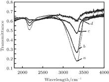
Raman scattering measurements indicate that the crystallization occurs in none of the samples studied. The IR absorption spectra of the films typically contain an Si– N stretching vibration in a range of 830 cm− 1– 860 cm− 1, Si– H stretching band at 2150 cm− 1, N– H stretching band at 3330 cm− 1– 3360 cm− 1, and N– H bending band at 1180 cm− 1. We did not observe any absorption assignable to Si– O bonds (460, 800, or 1070 cm− 1– 1090 cm− 1). Figure 1 shows the IR absorption spectra obtained from frustrated total internal reflection measurements, and SiNx:H layers are grown on specially prepared germanium prisms.
 | Fig. 1. IR absorption spectra of SiNx:H films grown at 160 ° C on Ge prisms and power densities of 0.05 (curve a), 0.1 (curve b), 0.2 (curve c), and 0.27 (curve d) W/cm2. |
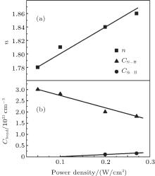
For quantitative calculations of the N– H and Si– H bond concentrations according to the Lambert– Beer law, we use the extinction coefficients cited from Ref. [1]: χ N− H = 1.06 × 10− 19 cm2 (absorption peak at 3340 cm− 1) and χ Si− H = 1.3 × 10− 19 cm2 (peak at 2150 cm− 1). The silicon-to-nitrogen atomic ratios evaluated from He+ backscattering data, differ only slightly from the stoichiometric values: at a pressure of 26 Pa an increase in power density from 0.05 W/cm2 to 0.3 W/cm2 led to an increase in Si/N ratio from 0.7 to 0.75. These data are typical for SiNx:H films without excessive silicon.[15]
The effects of discharge power density on the refractive index n and on the N– H and Si– H bond concentrations (Fig. 2) indicate that the plasma power has a significant influence on film properties. With increasing power density the refractive index, film density, and optical density of Si– N absorption all increase (Fig. 3). It correlates with the reduction of the hydrogen content (N– H bonds) and with the increase of Si– N bond number in the films.
 | Fig. 2. (a) Variations of refractive index n and (b) N– H and Si– H bond concentrations with power density of HF discharge for the films deposited at 160 ° C. |
The absorption Si– N peak not only changes strength but also shifts its wave number position from 872 cm− 1 to 850 cm− 1, as the power density increases (Fig. 3). The composition-induced peak shifts are usually discussed in view of the electronegativity of the film components.[16] Among the film forming chemical elements, N has the highest electronegativity and Si the lowest electronegativity, so the Si– N peak position is correlated to the N/Si ratio in the film. Also there is another model that explains the results obtained. The peak shifts of the Si– N absorption may be interpreted in terms of a charge-transfer model including hydrogen atoms.[17] From modeling the Si– N peak, wave numbers are found to be strictly linked to the Si– N bond lengths which depend on the partial charges on Si, and N or H atoms.
 | Fig. 3. Variations of (a) optical density of Si– N absorption, (b) films density, and (c) Si– N peak wave number with plasma power density. |
The biaxial stress σ in the film is calculated from Stoney’ s equation:

where E and ν are Young’ s modulus and Poisson’ s ratio of the substrate respectively, h is the substrate thickness, t is the film thickness, R is the radius of the curvature of the substrate with the film, and R0 is the radius of the curvature of the substrate. The equation is applied to the case where the thickness of the substrate is much larger than the film thickness.
Figure 4 shows the plot of mechanical stress versus discharge power density for SiNx:H films grown on single crystal silicon (111) substrates. The tensile stress is designated by a positive sign, and the compressive stress is denoted by a negative sign. It can be seen that with increasing the discharge power density, the tensile stress decreases. At a power density of 0.2 W/cm2, the stress changes sign, and the films grown at higher power densities are under compressive stress.
 | Fig. 4. Plot of mechanical stress versus plasma power density for films deposited on Si substrates at 160 ° C. The discharge frequency is 13.56 MHz. |
As is well known the SiNx:H film properties are mainly determined by low energy ion flux delivered to the film surface. The ion bombardment enhances surface diffusion, hydrogen desorption from the surface, and film structure formation. The increase in plasma power can modify the low-temperature film properties, i.e., their density, the concentration of Si– N bonds, and the refractive index n increase, but the concentration of bonded hydrogen decreases.
For our experimental conditions we perform the numerical calculations of capacitive HF (13.56 MHz) discharge characteristics by using the fluid model.[18] The system of equations includes the continuous equations for electron and ion densities and velocities, the continuous equation for electron energy, and the Poisson equation for electrical potential. The equations are solved self-consistently by the iterative method. The kinetic coefficients in the continuous equations such as an ionization rate, an electron attachment rate, a mobility, etc. are calculated by solving the kinetic equation for electron motion in two-term approximation. In the simulations the gas pressure is equal to 26 Pa and the input power varies from 0.05 W/cm2 to 0.2 W/cm2. The HF discharge operates in NH3/SiH4/Ar mixture. Several types of ions are considered. The resulting data have been described in detail elsewhere.[19] The results of the numerical calculation for the range of experimental parameters under investigation are shown in Table 1.
| Table 1. Results of the numerical calculations of HF (13.56 MHz) discharge characteristics at a pressure of 26 Pa in reactor. |
In Table 1 the computed ion energy, ion flux on the electrode and fraction of input power to the ion component of plasma are presented as a function of plasma power density. The simulation results show that the ion energy, ion flux, and ion component in input power increase rapidly with increasing the power density. The results of the numerical calculations do not explain the nature of the mechanical stress in films, but it is very useful to connect processes in the plasma with the properties of the films. Thus, the lower the ion energy and ion flux on the surface, the higher the hydrogen concentration and the value of the tensile stress are and the lower the density of the film is, as obtained experimentally and presented in Figs. 2, 3, and 4.
The obtained results are in good agreement with the results reported in the literature, where the influences of different deposition conditions (for discharge frequency range 0.1 MHz– 10 MHz) on the mechanical stress of silicon nitride layer formed by PECVD onto silicon substrates were studied by Claassen.[20] It was found that the mechanical stress of the as-deposited silicon nitride layer is a joint effect of the extent of ion bombardment and the deposition temperature on the hydrogen desorption rate. Deposited film shows a tensile stress character when the hydrogen desorption rate is thermally controlled (high temperature and high discharge frequency), whereas in the case of the ionbombardment-controlled hydrogen desorption rate the deposited film has a compressive stress. It was shown that for deposition at low temperature and low frequencies (up to 5 MHz) synthesized layers have compressive stresses. This is due to the influence of high energy argon ions causing implantation damage of films.
All the data presented are obtained for the films deposited by using HF plasma at the frequency of 13.56 MHz. Measurements of the intrinsic stress in silicon nitride films show that the stress quantity is not sufficient for the films applied to strained silicon photonics. It can be assumed that further increase in the frequency of the plasma will increase the tensile stress. Therefore, we use other process parameters, namely HF plasma at a frequency of 40.68 MHz. In all analyzed silicon nitride layers initial tensile stresses are observed in a range of 400 MPa– 70 MPa. The films grown at 250 ° C have higher mechanical stresses and their quantities are sufficient for the films applied to strained silicon photonics. The results in Figs. 5 and 6 show that heating films to 500 ° C changes the mechanical stress value significantly. Intrinsic stress starts to decrease from 350 ° C to 400 ° C.
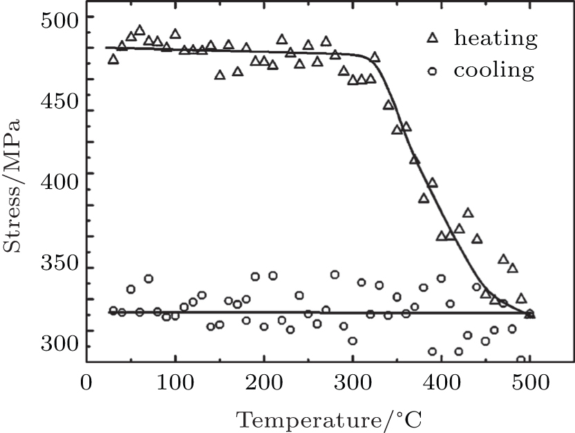 | Fig. 5. Variations of stress with temperature of SiNx:H films, grown at 16 ° C, through heating and subsequent cooling in Ar atmosphere. |
 | Fig. 6. Variations of stress with temperature of SiNx:H film, deposited at 250 ° C, through heating and subsequent cooling in Ar atmosphere. |
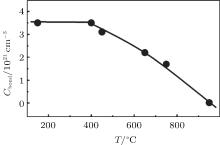
At 500 ° C a decrease is about 30% of the initial mechanical stress values. Further cooling does not affect the stress value in film. The observed effect is probably determined by the thermal destructions of Si– H and N– H bonds, release of hydrogen, changed film structure, and relaxed mechanical stress. The influence of thermal annealing on the hydrogen content in N– H bonds is presented on Fig. 7.
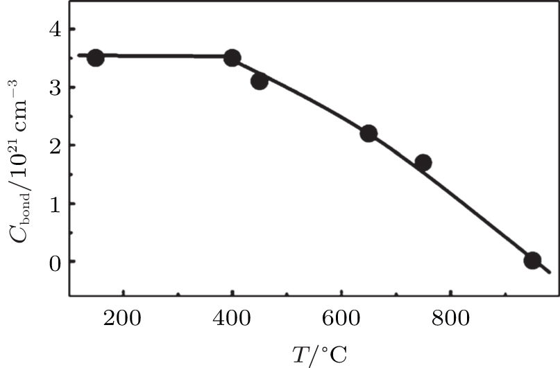 | Fig. 7. Variation of N– H concentration with temperature of a silicon nitride film as a result of annealing. Film is deposited at 160 ° C and plasma frequency of 40.68 MHz. |
At temperatures higher than 400 ° C, N– H bond distraction begins and, as a consequence, film experiences structural transformation and the stress value decreases. Our results (Fig. 7) are in good agreement with the results obtained by Claassen.[20] It is shown that due to annealing at temperatures above the deposition temperature the SiNx:H films are densified as a result of thermal destructions of Si– H and N– H bonds at 350 ° C– 400 ° C.
Also the influence of the plasma frequency on intrinsic mechanical stresses of SiNx:H films deposited by PECVD was investigated in Ref. [21]. At frequencies above 30 MHz, films tend to have tensile stresses. The authors relate this to the structural features, namely the introduction of hydrogen in the forms of N– H and Si– H bonds. Desorption of hydrogen is difficult at low temperatures in the absence of ion bombardment of the surface. Our data on the mechanical stresses in the films deposited at a discharge frequency of 40.68 MHz are consistent with those obtained in Ref. [21].
To explain the stresses in SiNx:H films deposited in a plasma with a frequency of 40.68 MHz, it is useful to consider the data of numerical calculations of the discharge. It is important to note that in our case the dominant component in gas mixture is argon, so the main contribution to the ion bombardment of the surface is made by argon ions. The effects of frequency variation in a range of 13.56 MHz– 54.4 MHz and at a low-pressure of 0.25 Torr (1 Torr = 1.33322 × 10² Pa) on capacitive coupled argon discharge have been investigated in Ref. [22]. Results of fluid model simulations under conditions (pressure and current density) close to our experimental parameters show that the self-bias potential and the ion energy of the plasma are significantly reduced with frequency increasing from 13.56 MHz to 40.68 MHz. The decrease of ion bombardment of the surface tends to form films with higher values of tensile stress.
The amorphous hydrogenated silicon nitride films are grown by the PECVD technique from SiH4, NH3, and Ar mixture. We investigate the effects of the plasma excitation frequency and power density on the film properties. At excitation frequency 13.56 MHz, with increasing plasma power density the tensile stress in film decreases and changes to compressive stress, also the refractive index, film density, and optical density of Si– N absorption increase. It correlates with the reduction of the hydrogen content (N– H bonds) and with the increase of Si– N bond content in the film. To understand the phenomenon, we calculate HF discharge characteristics by using the fluid approach. From the analysis of plasma discharge properties we find an evident correlation between ion flux parameters on the electrode and film intrinsic stress and properties. For films obtained at a frequency of 40.68 MHz the magnitude of the internal tensile stress reaches a value of 700 MPa which is sufficient for applications in silicon nanophotonics.
We are grateful to A.V. Panin for our discussion and I.V. Schweigert for the numerical calculations of capacitive plasma.
| 1 |
|
| 2 |
|
| 3 |
|
| 4 |
|
| 5 |
|
| 6 |
|
| 7 |
|
| 8 |
|
| 9 |
|
| 10 |
|
| 11 |
|
| 12 |
|
| 13 |
|
| 14 |
|
| 15 |
|
| 16 |
|
| 17 |
|
| 18 |
|
| 19 |
|
| 20 |
|
| 21 |
|
| 22 |
|