Analysis of recoverable and permanent components of threshold voltage shift in NBT stressed p-channel power VDMOSFET
Danković Danijel†a), Stojadinović Ninoslava), Prijić Zorana), Manić Ivicaa), Davidović Vojkana), Prijić Anetaa), Djorić-Veljković Snežanab), Golubović Snežanaa)
Department of Microelectronics, Faculty of Electronic Engineering, University of Nis, Serbia
Department of Mathematics, Physics and Informatics, Faculty of Civil Engineering and Architecture, University of Nis, Serbia

Corresponding author. E-mail: danijel.dankovic@elfak.ni.ac.rs

*Project supported by the Fund from the Ministry of Education, Science and Technological Development of the Republic of Serbia (Grant Nos. OI-171026 and TR-32026) and the Ei PCB Factory, Niš.

Abstract

In this study we investigate the dynamic recovery effects in IRF9520 commercial p-channel power vertical double diffused metal–oxide semiconductor field-effect transistors (VDMOSFETs) subjected to negative bias temperature (NBT) stressing under the particular pulsed bias. Particular values of the pulsed stress voltage frequency and duty cycle are chosen in order to analyze the recoverable and permanent components of stress-induced threshold voltage shift in detail. The results are discussed in terms of the mechanisms responsible for buildup of oxide charge and interface traps. The partial recovery during the low level of pulsed gate voltage is ascribed to the removal of recoverable component of degradation, i.e., to passivation/neutralization of shallow oxide traps that are not transformed into the deeper traps (permanent component). Considering the value of characteristic time constant associated with complete removal of the recoverable component of degradation, it is shown that by selecting an appropriate combination of the frequency and duty cycle, the threshold voltage shifts induced under the pulsed negative bias temperature stress conditions can be significantly reduced, which may be utilized for improving the device lifetime in real application circuits.

PACS: 66.30.Dn; 68.35.bg; 73.40.Qv; 82.33.Pt
Keyword: negative bias temperature instability; vertical double-diffused metal–oxide semiconductor; recoverable; permanent; degradation
1. Introduction

Negative bias temperature instability (NBTI) refers to the progressive shift of transistor parameters, such as threshold voltage (VT), transconductance, and absolute drain current. The NBTI has been found to occur mostly in p-channel metal– oxide semiconductor field-effect transistors (MOSFETs) operated at elevated temperatures (100  ° C– 250  ° C) under negative gate oxide fields in the range 2  MV/cm– 6  MV/cm.[110] From a relatively unknown problem in the past, NBTI has become an important reliability issue in metal– oxide semiconductor (MOS) technology primarily as a consequence of aggressive gate oxide scaling accompanied by less aggressive scaling of operating voltage. It is well known that this phenomenon is related to the stress-induced generation of oxide-trapped charge (Not) and interface traps (Nit). However, in spite of very extensive research during the last 15 years, a complete understanding of the physical mechanisms of NBTI remains elusive, and technology optimization to minimize NBTI is still a difficult problem.

Regardless of the fact that gate oxides in nanometre scale technologies have been continuously thinned down, the interest in thick oxides has not ceased due to widespread use of MOS technologies for the realisation of power devices. Power MOSFETs are widely used as fast switching devices in home appliances and automotive, industrial, and military electronics. It is important to note that the electric fields and temperatures applied to NBT stressing can be approached during the routine operations of power MOSFETs in many applications.[11] Thus, NBTI could be critical for reliable operations of power MOSFETs even though they have ultra-thick gate oxides, and the investigations of NBTI in power MOSFETs are of importance as well.[1115]

In this paper, we will present a consolidated discussion of the new results on threshold voltage instabilities, derived from the experiments on p-channel power VDMOS (vertical double diffused MOS) transistors subjected to static and pulsed NBT stressing. Power VDMOSFET is an attractive device for application in high-frequency switching power supplies due to its superior switching characteristics which enable operation in a megahertz frequency range.[16, 17] Also, power VDMOSFETs are widely used as the fast switching devices in home appliances and automotive, industrial, and military electronics.[11] In these applications gate bias during the operation switches between the “ high” and “ low” voltage levels, thus creating the pulsed stress conditions. A number of recent investigations of pulsed stress-induced NBTI have shown that unlike most reliability effects, NBTI-induced VT degradation recovers partly during the “ low” voltage levels. Namely, a portion of oxide-trapped charge and/or interface traps generated during the period fractions corresponding to the “ high” level may be neutralized and/or annealed during the period fractions corresponding to the “ low” level.[9, 1821] Earlier studies of pulsed NBTI mostly focused on modeling, including effects of stress conditions and recovery, as well as the frequency, duty cycle, and process dependencies.[1921] The objective of the present study is to analyze the recoverable and permanent components of NBTI and clarify the role of partial recovery of threshold voltage during the period fractions corresponding to the “ low” level of the pulsed stress voltage in overall NBTI. Specifically, this study is aimed at investigating the possibility of finding a suitable combination of stress voltage frequency and duty cycle that would result in a minimal stress-induced degradation, thus yielding the optimal device lifetime.

2. Experimental procedure

Devices used in this study were commercial p-channel power VDMOSFETs IRF9520 with current and voltage ratings of 6.8  A and 100  V respectively, encapsulated in TO-220 plastic cases. Devices were built in standard silicon-gate technology with 100-nm thick gate oxide, and had the initial threshold voltage VT0 = − 3.6  V.[22] Owing to the thick gate oxide, accelerated NBT stressing of these devices required gate stress voltage amplitudes even over − 40  V, which exceeded capabilities of commonly used signal voltage sources.[2325] For these reasons it was necessary to develop a system for NBT stress and measurements on power VDMOSFETs. Furthermore, in order to investigate NBTI effects it was necessary to develop appropriate measurement technique.[2630] The current– voltage (IV) method is commonly employed in the literature. Using this method, the stress voltage, either static or pulsed, is removed from the device to perform measurement, and the threshold voltage is determined from the measured transfer IV characteristic. In order to minimize the recovery effects on threshold voltage value, it is essential to perform the measurement as fast as possible. Having in mind the above mentioned, we have recently developed stress and measurement technique based on cost-effective switching circuit, which provides reasonable compromise between stress and measurement requirements and is suitable for NBT stress and measurements on VDMOS transistors.[31, 32]

Our measurement technique has been verified by a series of NBTI tests on several devices.[3133] As an example, figure  1 shows measured transfer IV characteristics for a VDMOS device subjected to 24  h of the pulsed NBT stress at VG = − 45  V, T = 175  ° C, f = 18.82  kHz, DTC = 94.12%. During the 24-h test, the total of 37 interim measurements were performed according to the predefined timeline, but for simplicity only a few transfer IV characteristics are shown. The transfer IV characteristics were measured at a drain voltage value of 100  mV, so the device was kept in the linear region of operation. Gate voltage was swept from − 2  V to − 4.75  V, in steps of − 50  mV. As can be seen, the characteristics are shifted along the gate voltage axis toward the higher voltage values, while their slope slightly decreases, pointing to the generation of oxide trapped charge and interface traps induced by NBT stress, which is well established in the literature.[12, 34, 35] The proposed measurement technique provides the full range IV characteristics that can be used to determine threshold voltage and extract some other important device parameters, such as channel carrier mobility and transconductance. In this paper we will focus our discussion on threshold voltage values, which were calculated from the measured transfer IV characteristics using the second derivative method.[36]

Fig.  1. Measured transfer IV characteristics of p-channel power VDMOSFETs during the pulsed (VG = − 45  V, T = 175  ° C, f = 18.82  kHz, DTC = 94.12%) NBT stressing.

3. Results and discussion

In a preliminary experiment, ten sets of p-channel devices are stressed at 175  ° C for 24  h under the static and pulsed NBT stress conditions. For the static NBT stress, a negative DC voltage of − 45  V is applied to the gate, whereas the drain and source terminals are grounded. For the pulsed NBT stress, device stressing is performed by applying a negative pulsed voltage of − 45  V (with a base level of 0  V) to the gate, while the drain and source terminals are grounded. Five different frequencies and five different duty cycles (DTCs) of pulsed negative voltage are used in the experiment as given in Table  1, where D1– D9 denote different groups of devices under test (DUT). This choice of stress parameters is found to be convenient to investigate the dependences of stress-induced threshold voltage shift (Δ VT) on frequency and duty cycle.

Table 1. Pulsed bias conditions applied for NBT stressing of p-channel power VDMOSFETs. The measured transfer IV characteristics of one of these DUT are shown in Fig.  1.

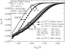
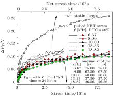
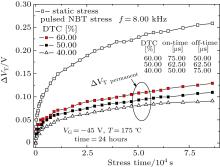
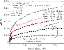
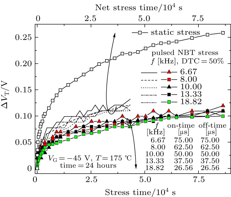
Three characteristic sets of data (at five different frequencies for DTC = 50% and for three DTCs at f = 8.00  kHz and 18.82  kHz) for the time dependences of threshold voltage shift during the pulsed and static NBT stressing of IRF9520 p-channel VDMOSFETs are shown in Figs.  2– 4, respectively. The literature results for the frequency dependence of pulsed NBTI-related degradation appear rather inconsistent.[37] In some papers only a weak frequency dependence of NBT degradation in the range 100  Hz < f < 100  kHz is reported, [19, 38] whereas the others show a monotonic decrease of stress-induced Δ VT with frequency decreasing.[39, 40] In our case, the results shown in Fig.  2 suggest that Δ VT under the pulsed NBT stress conditions becomes more pronounced with frequency increasing. This dependence is not so clearly pronounced due to rather narrow frequency range. On the other hand, it is clearly noticeable that the pulsed NBT stressing generally gives rise to low shifts as compared with static stressing. The reason for the observed lower shifts in the case of the pulsed NBT stress can be found to lie in two factors associated with the nature of pulsed stressing itself. The first factor is assessed by taking into account that “ stress time” in Fig.  2 refers to the total time, which includes fractions of the periods corresponding to both “ high” and “ low” levels of the pulsed gate voltage applied. However, the devices are stressed only during the fraction of period corresponding to the “ high” voltage level (on-time), so the actual or net stress time in the cases of pulsed stressing is significantly shorter (and the resulting stress-induced threshold voltage shifts appear lower) than in the case of static one. In accordance with this thinking, in Fig.  2 we can also see the results for the threshold voltage shifts versus net stress time, where the net stress time in the case of pulsed stressing is calculated by multiplying the total stress time with duty cycle (50% in this case). These results show that for corresponding values of the net stress time, the stress-induced threshold voltage shifts under the static stress remain much higher than in the case of pulsed NBT stress. Also, we can see that the difference between the degradation caused by the static NBT stress and that by pulsed NBT stress increases with stress time increasing. This clearly indicates that Δ VT time dependences in Fig.  2 have been affected by the other factor, i.e., partial recovery of threshold voltage during the period fractions corresponding to the “ low” level (off-time) of the pulsed stress voltage, which is frequently referred to as dynamic recovery.[9, 1821] The results of our previous study, which focused on a dynamic recovery phenomenon in VDMOS devices IRF9520, points to the existence of characteristic time constant (25-μ s) related to the recoverable and permanent components of stress-induced degradation.[33] It was found that 25-μ s off-time of the pulsed stress voltage is sufficient to completely remove the recoverable component of degradation created during the preceding pulse on-time.[33] The pulse off-time values in the cases of experimental data shown in Fig.  2 are longer than 25  μ s, so we can conclude that in this case only the slowly relaxing or permanent component can contribute to the resulting Δ VT.
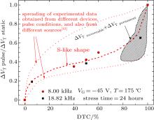
Fig.  2. Threshold voltage shifts during static and pulsed NBT stress at different frequencies, DTC = 50%.

Similar discussion is applied to the results in Fig.  3, which shows the time dependences of threshold voltage shift during the pulsed NBT stressing for different duty cycles at f = 8.00  kHz. As can be seen, the off-times in this case are also longer than 25  μ s, so the Δ VT also consists only of the permanent component. The situation in Fig.  4 (f = 18.82  kHz) however differs from that in Fig.  3: only permanent component of Δ VT is present in the groups of devices stressed at DTC = 5.88% and 50% (with corresponding pulse off-time values equal to 50  μ s and 26.56  μ s, respectively), whereas both recoverable and permanent components contributed to Δ VT in devices stressed at DTC = 94.12% (off-time equals to 3.12  μ s). It should be mentioned that the particular values of frequency and duty cycle for this experiment are chosen in connection with our previous studies, [3133] so we could proceed with studying the recoverable and permanent components of Δ VT during the NBT stressing of p-channel power VDMOSFETs.

Fig.  3. Threshold voltage shifts during static and pulsed NBT stress at different duty cycles, f = 8.00  kHz.

Fig.  4. Threshold voltage shifts during static and pulsed NBT stress at different duty cycles, f = 18.82  kHz.

3.1. Duty cycle dependence

Figure  5 shows the duty cycle dependence of stress-induced Δ VT under pulsed stress conditions, normalized to Δ VT induced by the static stress. It is well established in the literature that the shape of duty cycle-dependent data shows very large spread when pulsed stress data are normalized to static stress ones.[19, 41] The pulsed/static data ratio as reported by various groups shows spread in a range of 0.3– 0.8 at 50% duty cycle, and especially huge scattering is observed for higher DTC close to the static stress. As discussed in Refs.  [4], [9], and [41], the spread in data from different sources can be ascribed to differences in device quality, preexisting bulk trap density, measurement approach (on-the-fly or stress-measure-stress method) and/or differences in measurement speed, as well as to the difference between the contribution of oxide trapped charge and that of interface traps. Our experimental data shown in Figs.  2– 4, as well as the conclusions from our previous investigation, [33] are in line with these findings. Namely, the slowly relaxing or permanent component of Δ VT in p-channel power VDMOSFETs is dependent on frequency and duty cycle, and this is more pronounced at lower frequencies and higher values of duty cycles as graphically indicated in Fig.  5. That is why the modeling of threshold voltage shifts for pulsed NBT stress represents a challenge. Threshold voltage is widely accepted as a well-suited parameter that can be used as a degradation monitor for the lifetime estimation. In order to estimate the lifetime of investigated VDMOSFETs the following dependence of Δ VT on the stress field (E), time (t), and temperature (T) during the static NBT stress has earlier been derived:[34, 42, 43]

where A is a constant, Ea is the activating energy, and k is the Boltzmann constant. However, considering the fact that power VDMOSFETs are widely used as the fast switching devices in various applications, [11] it may be important to include the frequency and duty cycle dependences in the above model as expressed below

(2)

where F1 and F2 are functions accounting for the frequency and duty cycle dependencies, respectively. However, taking into account the simultaneous influences of permanent and recoverable components on the Δ VT at some frequencies and for some values of duty cycle, it is not so easy to separate functions F1 and F2 and their individual influences on the shape of Δ VT. Trying to clarify the above considerations, the rest of the paper will focus on the influences of permanent and recoverable components on Δ VT during the pulsed NBT stressing.

Fig.  5. Curves of pulsed NBTI degradation (normalized to static stress) versus pulse duty cycle. The graphical illustration of the area with recoverable and permanent components of degradation is indicated as well.

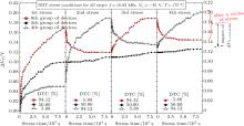
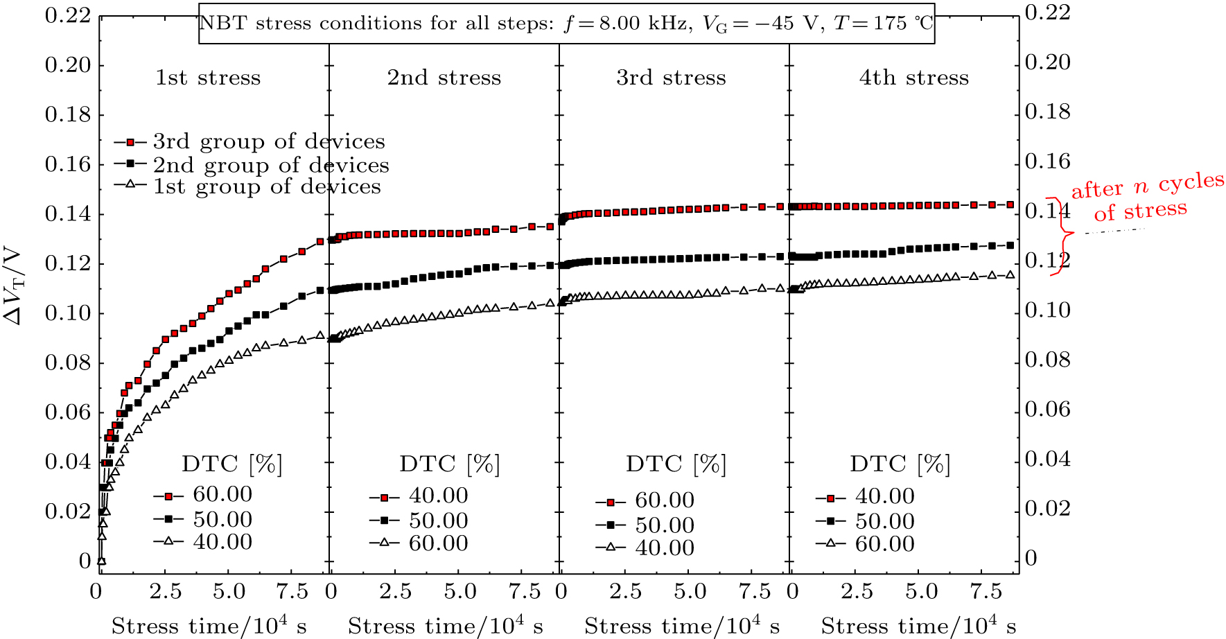
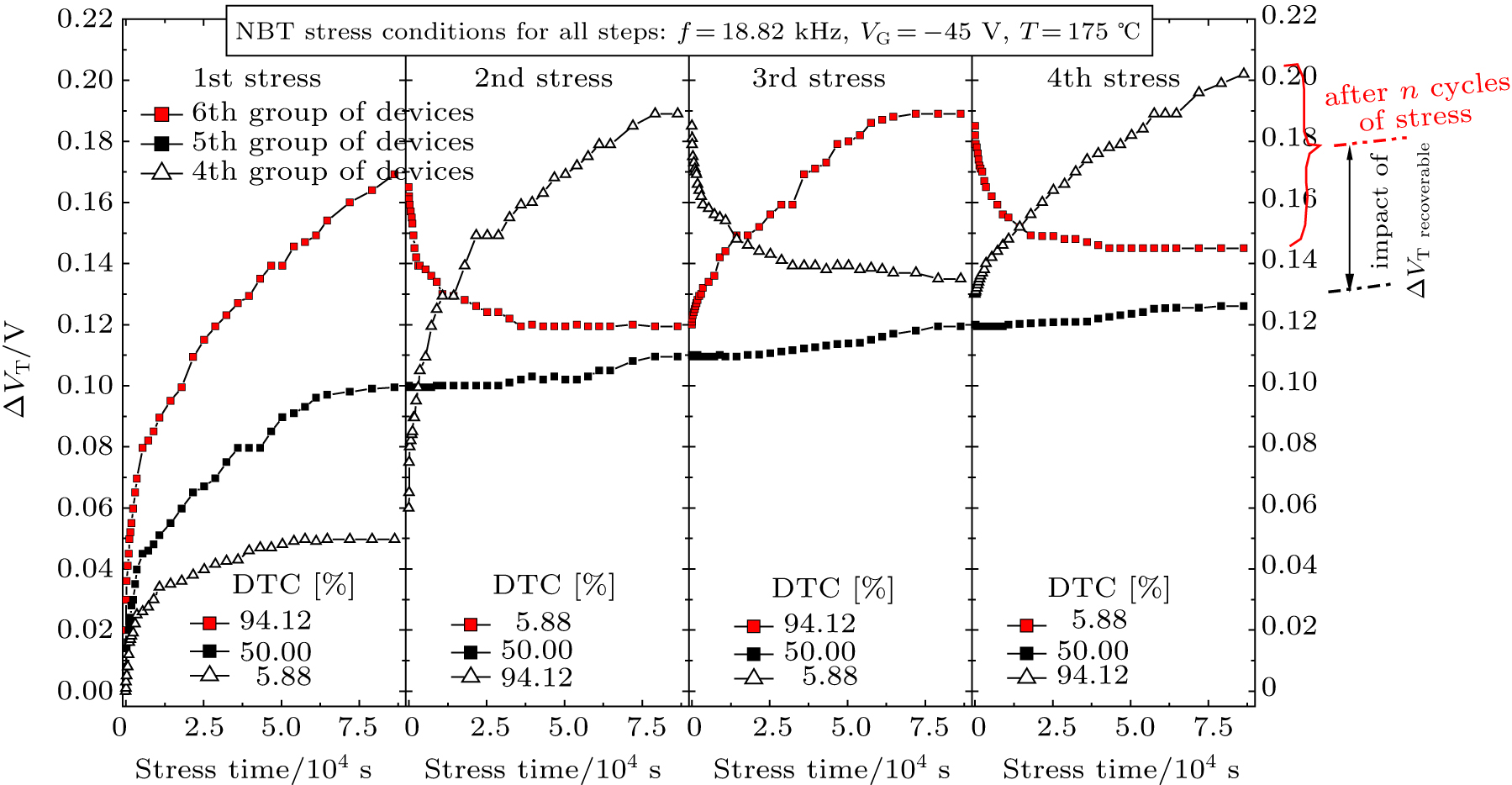
3.2. Permanent and recoverable components of Δ VT

Most of NBTI studies have focused on investigations under specific static and/or pulsed stress conditions. However, in many applications devices can be used in multiple modes and/or under varying conditions, which means at variable frequencies, duty cycles, gate voltages, etc., so it appears interesting to examine what will happen if previously stressed devices are stressed again, but under different pulsed NBT stress conditions. Accordingly, devices from previous experiment (results shown in Figs.  3 and 4) are re-stressed three more times, and the overall experiment is managed as shown in Table  2. As in the preliminary experiment, devices are stressed with − 45  V at 175  ° C, and the duration of each stressing step is 24  h, so during the 4-step stress sequence devices are stressed 96 h and all groups of devices have identical net stress times (48  h). Devices are characterized by the same intermittent measurements as in previous experiment.

Table 2. Pulsed bias conditions applied for 4-step NBT stressing of p-channel power VDMOSFETs. The results for 1st stress are shown in Figs.  3 and 4.

The threshold voltage shifts observed in devices subjected to a stressing sequence described by Table  2, are shown in Figs.  6 and 7. As can be seen in Fig.  6, first NBT stress creates different VT shifts in all groups of devices, depending on DTC. The VT shift in the first stress step, observed in the 2nd group of devices, proceeds in rather continuous manner throughout all other steps. Though, it should be noted that Δ VT is almost saturate in the first stress step and slightly increases over the next three steps. Qualitatively similar behavior can be seen in the 1st and 3rd groups of devices during all stress steps, but VT shifts are somewhat higher at DTC =   60% and somewhat lower at DTC =   40%. As a result, the differences between Δ VT values obtained in three groups of devices after each even number of steps (which means at equal net stress time) have tended to shrink and may even disappear after a large number of stress steps. The differences in Δ VT behavior between three groups of devices are rather small due to relatively small variations in duty cycle (± 10% from the intermediate value of 50%).

Fig.  6. Threshold voltage shifts during the 4-step sequence of pulsed NBT stressing (VG = − 45  V, T = 175  ° C, f = 8.00  kHz) at different duty cycles.

Fig.  7. Threshold voltage shifts during the 4-step sequence of pulsed NBT stressing (VG = − 45  V, T = 175  ° C, f = 18.82  kHz) at different duty cycles.

However, as can be seen in Fig.  7, huge differences in Δ VT behavior between the groups are observed when significant variations in duty cycle (about 44% from the intermediate value of 50%) are applied. The first NBT stress creates quantitatively different VT shifts in all groups of devices, depending on DTC, while important qualitative differences among three groups appear to start from the second stress step. The Δ VT values in the 5th group of devices behave in a similar manner to those in the first three groups (Fig.  6), which could be expected given that the 5th group is stressed at DTC = 50%. Actually, Δ VT behavior in the 5th group is almost identical to that in the 2nd group shown in Fig.  6, though the observed changes are slightly less pronounced. On the other hand, the initial VT shifts in devices from the 4th and 6th groups (DTC = 5.88% and 94.12%, respectively) created in the first stress step do not behave in the same manner and suffered remarkable changes during the subsequent stress steps. Threshold voltage in devices from the 6th group continuously decreases during the 2nd stress step. The decrease is most rapid immediately after the first stress, but gradually slows down and finally reaches a saturate state. This behavior of threshold voltage largely resembles the annealing of p-channel power VDMOSFETs, which was discussed in detail in our previous paper.[44] Considering the on-time/off-time ratio for the 6th group of devices, as well as the value of duty cycle during the 2nd stress step (5.88%) and the shape of the curves shown in Fig.  7, we can conclude that the 2nd stress step leads to the annealing of oxide trapped-charge and interface traps rather than to their creation. As is well known, the changes in device threshold voltage during the NBT stress are attributed to the generation of oxide-trapped charge and interface traps due to stress-initiated electrochemical processes and reactions involving oxide and interface defects, holes, and various species (H, H2, H+ , OH, H2O, H3O+ ) associated with the presence of hydrogen as a common impurity in MOS devices.[13, 5, 12, 4446] Buildup of oxide charge under the high negative oxide field can be explained by hole trapping at near-interface oxygen vacancy defects:[42]

or by the dissociation of weak Si– H bonds near the interface by high electric field:[47]

The above oxide charge could be transformed into interface traps, [42] but the buildup of interface traps is more likely to occur due to dissociation of weak interfacial Si– H bonds by high electric field:[1, 3]

The released highly reactive neutral hydrogen atoms can also dissociate the Si– H bonds at the interface or in the oxide near the interface:[1, 3]

leading to the creation of additional interface traps or positively charged oxide defects. Alternatively, hydrogen atoms can react with an abundance of holes from the substrate to form ions:[48]

which afterwards, drifting away from interface toward the gate under the negative oxide field, can dissociate the Si– H bonds in the gate oxide near the interface:[1, 48]

leading to the creation of additional positively charged oxide defects.

The H2 molecules released in reaction  (6) at interface, and reactions  (7) and (9) in the vicinity of interface diffuse more deeply into the oxide and can be cracked at positively charged oxide traps:[49]

Neutral hydrogen released in reaction  (10) can take part in forward reactions  (6) and (7), as well as in reverse reactions  (4) and (5), rounding up the chain of reactions  (4)– (10).

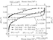
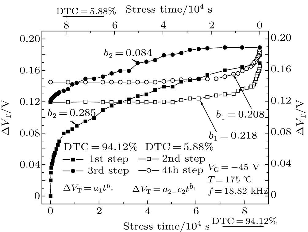
In terms of the model described by the above reactions, oxide-trapped charge (Not) and interface traps (Nit) are created through the reactions  (3)– (7) and (9) during the on-time in each cycle of pulsed NBT stressing. The on-time for the 6th group of devices in the 2nd stress step is rather short (3.12  μ s), so the buildup of Not and Nit is significantly lower than during the first stress. In addition, the off-time for this group of devices in the 2nd stress step (50  μ s) is much longer than the on-time, so the recovery through the reverse reactions  (4)– (7) and (9) (which lead to the neutralization of oxide-trapped charge and the passivation of interface traps) becomes more significant than during the first stress step. As a consequence of the above two phenomena in the 2nd stress step (reduced degradation and enhanced recovery as compared with the first stress) the initial degradation, which is created in the 6th group during the first stress step, tends to be annealed during the second stress. The amount of recovery depends on the off-time, as well as on the status of the gate oxide and SiO2– Si interface found immediately after the first stress, including the densities of stress-induced oxide-trapped charges and interface traps and their spatial and energy distributions, the number of potential trapping sites and quantities of reacting species available, including new defects possibly created by preceding stress. It is important to note that the main part of recovery during the off-time can be ascribed primarily to the recoverable component of degradation, which actually means passivation/neutralization of shallow oxide traps that are not transformed into deeper traps (permanent component).[50, 51] As can be seen in Fig.  7, Δ VT value for the 6th group of devices during the 2nd stress step approaches to the value of Δ VT for the 5th group, but does not reach it. This clearly indicates that contribution of the recoverable component to overall degradation in the 6th group of devices has not been completely removed during the 2nd stress step. Moreover, during the 3rd and 4th stress step Δ VT for the 6th group of devices shows qualitatively the same behavior as during the 1st and 2nd stress step, but all changes are slower and lower. As a result, after each even number of step some shallow oxide traps are permanently transformed into deeper traps. This can be clearly seen in Fig.  8, which shows the threshold voltage shifts observed in the 6th group of devices during the 4-step sequence of pulsed NBT stressing. The curves of Δ VT versus time shown in Fig.  8 can be fitted by the following equation during the odd stress steps:[34, 42, 43]

and by the following one during the even stress steps:[52]

where a1, b1, a2, b2, and c2 are the fitting parameters. Namely, the power-law time evolution is a reasonable approximation for modeling the threshold voltage shift as a function of time. It should be noted here that the behavior of threshold voltage shifts during the even stress step is dominantly shaped by the recovery (i.e. annealing) phenomenon, so we use Eq.  (12), which is the characteristic function for annealing. As can be seen, the threshold voltage quickly recovers in the early stage of the 2nd stress step, but major portion of the shift induced by the first stress step is restored when repeating the stress during the 3rd stress step, though not so quickly. The change in Δ VT tends to be less pronounced in each new repetition, which can be clearly seen from the values of parameters b1 and b2, indicating that Δ VT will tend to be saturate after large number of stress steps.

Fig.  8. Threshold voltage shifts during the 4-step sequence of pulsed NBT stressing (VG = − 45  V, T = 175  ° C, f = 18.82  kHz) for the 6th group of devices.

It is important to note that Δ VT for the 4th group of devices shows quantitatively and qualitatively the same behavior as for the 6th group, where Δ VT behaviors observed in the 4th group of devices during the 2nd, 3rd, and 4th stress steps corespond to Δ VT behaviors observed in the 6th group of devices during the 1st, 2nd, and 3rd stress steps, respectively. This is quite understandable because the NBT stress conditions are the same during the corresponding steps. As a consequence, one may expect that Δ VT will be saturated after a large number of stress steps in both groups of devices. However, Δ VT values in both groups of devices remain above Δ VT in the 5th group, pointing out to the transformation of the recoverable component of degradation into a more permanent one. These results have clearly shown that, if the p-channel power VDMOSFETs are exposed to the pulsed NBT stress with pulse off-time shorter than 25  μ s at any stage of their operation, the resulting instabilities could be more serious than those found in devices exposed to pulsed NBT stress with pulse off-time longer than 25  μ s, regardless of the same net stress time. Accordingly, we can conclude that by selecting an appropriate combination of the frequency and duty cycle, the Δ VT induced under the pulsed NBT stress conditions can be significantly reduced, which as a result may lead to the improvement in device lifetime. Though, it should be noted that actual choice of optimal frequency and DTC depends on circuit requirements.

Existing studies about pulsed NBTI show a relation between Δ VT and DTC, having the typical S-like shape[41] as illustrated in Fig.  5. The reason for this shape has not yet been completely explained, but many research groups provide a good fit with experimental data. The above considerations clearly indicate that functions F1 and F2 in Eq.  (2), which are used to account for the frequency and DTC dependences, respectively, are mutually dependent at some frequencies and for some values of duty cycles. Accordingly, threshold voltage shift models for pulsed NBT stressed VDMOSFETs need to be modified at lower frequencies and for higher values of duty cycle as a consequence of creation of the slowly relaxing or permanent component of degradation, which appears due to the transformation of some shallow oxide traps into the deeper ones.

4. Conclusions

The dynamic recovery effects in p-channel power VDMOSFETs subjected to NBT stressing under the particular pulsed bias conditions are analyzed. Particular values of the pulsed stress voltage frequency and duty cycle are chosen to analyze the recoverable and permanent components of degradation and assess the role of partial recovery of threshold voltage during the period fractions corresponding to the “ low” level of the pulsed stress voltage in overall NBTI. The results are discussed in terms of the mechanisms represented by several electrochemical reactions, which include hole trapping and dissociation of Si– H bonds under the high electric field, as well as some other reactions involving both oxide and interface defects and hydrogen-related species. Most of these reactions can occur in either forward or reverse directions, leading to the buildup of oxide charge and interface traps or to their neutralization/passivation, which is utilized to explain partial recovery during the low level of pulsed gate voltage. This recovery depends on off-time, as well as on gate oxide and SiO2– Si interface status found immediately after the stress, including the densities of stress-induced oxide-trapped charges and interface traps and their spatial and energy distributions. Our results have clearly shown that, if the p-channel power VDMOSFETs are exposed to pulsed NBT stress with pulse off-time shorter than 25  μ s at any stage of their operation, the related instabilities could be more serious than those found in devices exposed to pulsed NBT stress with pulse off-time longer than 25  μ s, regardless of the same net stress time. It is further shown that by selecting an appropriate combination of the frequency and duty cycle, the Δ VT induced under the pulsed NBT stress conditions can be significantly reduced, thus leading to the improvement in device lifetime. Though, this is just an option, as the actual choice of optimal operation frequency and DTC depends on circuit requirements.

Reference
1 Schroder D K and Babcock J A 2003 J. Appl. Phys. 94 1 DOI:10.1063/1.1567461 [Cited within:5]
2 Stathis J H and Zafar S 2006 Microelectron. Reliab. 46 270 [Cited within:1]
3 Ogawa S, Shimaya M and Shiono N 1995 J. Appl. Phys. 77 1137 DOI:10.1063/1.358977 [Cited within:3]
4 Mahapatra S, Goel N, Desai S, Gupta S, Jose B, Mukhopadhyay S, Joshi K, Jain A, Islam A E and Alam M A 2013 IEEE Trans. Electron Dev. 60 901 DOI:10.1109/TED.2013.2238237 [Cited within:1]
5 Alam M A and Mahapatra S A 2005 Microelectron. Reliab. 45 71 [Cited within:1]
6 Grasser T, Aichinger T, Pobegen G, Reisinger H, Wagner P J, Franco J, Nelhiebel M and Kaczer B 2011Proceedings of the 49th IEEE International Reliability Physics Symposium(IRPS2011), ed. Stathis J S (Monterey: EDS and RS of the IEEE) 6A. 2. 1 [Cited within:1]
7 Zhang Y, Pu S, Lei X Y, Chen Q, Ma X H and Hao Y 2013 Chin. Phys. B 22 117311 DOI:10.1088/1674-1056/22/11/117311 [Cited within:1]
8 Karim N M, Manzoor S and Soin N 2013 Renewable and Sustainable Energy Reviews 26 776 DOI:10.1016/j.rser.2013.06.004 [Cited within:1]
9 Alam M A 2003 Technical Digest of the IEDM 345 [Cited within:3]
10 Zhang Y, Zhuo Q Q, Liu H X, Ma X H and Hao Y 2014 Chin. Phys. B 23 057304 DOI:10.1088/1674-1056/23/5/057304 [Cited within:1]
11 Gamerith S and Polzl M 2002 Microelectron. Reliab. 42 1439 DOI:10.1016/S0026-2714(02)00165-8 [Cited within:4]
12 Stojadinović N, Danković D, Djorić-Veljković S, Davidović V, Manić I and Golubović S 2005 Microelectron. Reliab. 45 1343 [Cited within:2]
13 Alwan M, Beydoun B, Ketata K and Zoaeter M 2007 Microelectron. Reliab. 47 1406 DOI:10.1016/j.microrel.2007.07.096 [Cited within:1]
14 Beydoun B, Alwan M, Ketata K and Zoaeter M 2008 J. Active Passive Electron. Dev. 3 77 [Cited within:1]
15 Tallarico A N, Magnone P, Barletta G, Magrì A, Sangiorgi E and Fiegna C 2014 IEEE Trans. Dev. Mater. Reliab. 14 657 DOI:10.1109/TDMR.2014.2308580 [Cited within:1]
16 Baliga B J 1987 Modern Power Devices New York John Wiley [Cited within:1]
17 Benda V, Gowar J and Grant D A 1999 Power Semiconductor Devices New York John Wiley [Cited within:1]
18 Fernández R, Kaczer B, Nackaerts A, Demuynck S, RodrÍguez R, Nafria M and Groeseneken G 2006 Technical Digest of the IEDM 1 [Cited within:2]
19 Mahapatra S, Islam A E, Deora S, Maheta V D, Joshi K, Jain A and Alam M A 2011Proceedings of the 49th Ann. Int. Reliability Physics Symp. (IRPS2011), ed. Stathis J S (Monterey: EDS and RS of the IEEE) 614 [Cited within:3]
20 Reisinger H, Grasser T, Ermisch K, Nielen H, Gustin W and Schlünder C 2011Proceedings of the 49th Ann. Int. Reliability Physics Symp. (IRPS2011), ed. Stathis J S (Monterey: EDS and RS of the IEEE) 597 [Cited within:1]
21 Desai S, Mukhopadhyay S, Goel N, Nanaware N, Jose B, Joshi K and Mahapatra S 2013Proceedings of the 51th Ann. Int. Reliability Physics Symp. (IRPS2013), ed. Stathis J S (Anaheim: EDS and RS of the IEEE) XT. 2. 1 [Cited within:3]
22 “IRF9520N, ” Data sheet, International Rectifier 1998. [online] Available: http://www.irf.com [Cited within:1]
23 “High amplitude arbitrary/function generator simplifies measurement in automotive semiconductor, scientific and industrial applications, ” Application Note, Tektronix, Inc. 2008. [online] Available: http://www.tektronix.com/afg3000 [Cited within:1]
24 “Agilent 4156C precision semiconductor parameter analyzer“, Data sheet, Agilent Technologies Inc. 2009, p.  5. [online] Available: http://www.agilent.com [Cited within:1]
25 “Agilent 33502A 2-channel 50 Vpp isolated amplifier“, Data sheet, Agilent Technologies Inc. 2009. [online] Available: http://www.agilent.com [Cited within:1]
26 Reisinger H, Brunner U, Heinrigs W, Gustin W and Schlunder C 2007 IEEE Trans. Dev. Mater. Reliab. 7 531 DOI:10.1109/TDMR.2007.911385 [Cited within:1]
27 Li M F, Huang D, Shen C, Yang T, Liu W J and Liu Z 2008 IEEE Trans. Dev. Mater. Reliab. 8 62 DOI:10.1109/TDMR.2007.912273 [Cited within:1]
28 Brisbin D and Chaparala P 2009 IEEE Trans. Dev. Mater. Reliab. 9 115 DOI:10.1109/TDMR.2009.2021257 [Cited within:1]
29 Schlunder C, Hoffmann M, Vollertsen R, Schindler G, Heinrigs W, Gustin W and Reisinger H 2008Proceedings of the 46th International Reliability Physics Symposium(IRPS2008), ed. Stathis J S (Pheonix: EDS and RS of the IEEE) 79 [Cited within:1]
30 Grasser T, Wagner P J, Hehenberger P, Goes W and Kaczer B 2008 IEEE Trans. Dev. Mater. Reliab. 8 526 DOI:10.1109/TDMR.2008.2002353 [Cited within:1]
31 Prijić A, Danković D, Vračar Lj, Manić I, Prijić Z and Stojadinović N 2012 Meas. Sci. Technol. 23 1 [Cited within:3]
32 Manić I, Danković D, Prijić Z, Prijić A and Stojadinović N 2014 Informacije MIDEM, Journal of Microelectronics, Electronic Components and Materials 44 280 [Cited within:1]
33 Danković D, Stojadinović N, Prijić Z, Manić I and Prijić A 2014Proceedings 29th International Conference on Microelectronics(MIEL), ed. Stojadinović N (Belgrade: EDS of the IEEE) 297 [Cited within:5]
34 Danković D, Manić I, Djorić-Veljković S, Davidović V, Golubović S and Stojadinović N 2009 Microelectronic and Mechanical SystemsTakahata K (Boca Raton, IN-TECH Press) 19. 319 [Cited within:3]
35 Stojadinović N, Manić I, Danković D, Djorić-Veljković S, Davidović V, Prijić A, Golubović S and Prijić Z 2014 Bias Temperature Instability for Devices and Circuits Grasser T New York Springer533 [Cited within:1]
36 Ortiz-Conde A, García Sánchez F, Liou J, Cerdeira A, Estrada M and Yue Y 2002 Microelectron. Reliab. 42 583 [Cited within:1]
37 Nigam T 2008 IEEE Trans. Dev. Mater. Reliab. 8 72 DOI:10.1109/TDMR.2008.918314 [Cited within:1]
38 Li M F, Chen G, Shen C, Wang X P, Yu H Y, Yeo Y C and Kwong D L 2004 Jpn. J. Appl. Phys. 43 7807 DOI:10.1143/JJAP.43.7807 [Cited within:1]
39 Ma X H, Cao Y R and Hao Y 2010 Chin. Phys. B 19 117308 DOI:10.1088/1674-1056/19/11/117308 [Cited within:1]
40 Zhu B, Suehle J S, Chen Y and Bernstein J B 2002Proceedings IEEE IRW FINAL REPORT 125 [Cited within:1]
41 Mahapatra S 2014 Bias Temperature Instability for Devices and Circuits Grasser T New York Springer349 [Cited within:3]
42 Stojadinović N, Manić I, Davidović V, Danković D, Djorić-Veljković S, Golubović S and Dimitrijev S 2005 Microelectron. Reliab. 45 115 [Cited within:4]
43 Stojadinović N, Djorić-Veljković S, Davidović V, Manić I and Golubović S 2001in Proceedings of the 5th International Conference on Telecommunications in Modern Satellite, Cable and Broadcasting Services(TELSIKS2001), ed. Milovanović B (Niš IEEE and Faculty of Electronic Engineering) 395 [Cited within:2]
44 Manić I, Danković D, Djorić-Veljković S, Davidović V, Golubović S and Stojadinović N 2009 Microelectron. Reliab. 49 1003 [Cited within:2]
45 Danković D, Manić I, Davidović V, Djorić-Veljković S, Golubović S and Stojadinović N 2007 Microelectron. Reliab. 47 1400 DOI:10.1016/j.microrel.2007.07.022 [Cited within:1]
46 Tan S, Chen T, Ang C and Chan L 2003 Appl. Phys. Lett. 82 269 DOI:10.1063/1.1537053 [Cited within:1]
47 Dimitrijev S, Golubović S, Župac D, Pejović M and Stojadinović N 1989 Solid-State Electron. 32 349 DOI:10.1016/0038-1101(89)90122-6 [Cited within:1]
48 Fleetwood D M 2002 Microelectron. Reliab. 42 523 [Cited within:2]
49 Ristić G, Pejović M and Jakšić A 2000 J. Appl. Phys. 87 3468 [Cited within:1]
50 Duan M, Zhang J F, Ji Z, Zhang W D, Kaczer B, Gendt S D and Groeseneken G 2013 IEEE Trans. Electron Dev. 60 413 DOI:10.1109/TED.2012.2223702 [Cited within:1]
51 Gao Y, Ang D S, Bersuker G and Young C D 2013 IEEE Electron Dev. Lett. 34 351 DOI:10.1109/LED.2013.2242041 [Cited within:1]
52 Tsujikawa S, Mine T, Watanabe K, Shimamoto Y, Tsuchiya R, Ohnishi K, Onai T, Yugami J and Kimura S 2003Proceedings of the 41st Annual International Reliability Physics Symposium. (IRPS2003), ed. Snyder E S (Dallas: EDS and RS of the IEEE) 183 [Cited within:1]