Zheng Qi-Wen, Cui Jiang-Wei†, Zhou Hang, Yu De-Zhao, Yu Xue-Feng, Lu Wu, Guo Qi, Ren Di-Yuan. Analysis of functional failure mode of commercial deep sub-micron SRAM induced by total dose irradiation. Chinese Physics B, 24(10): 106106
Permissions
Analysis of functional failure mode of commercial deep sub-micron SRAM induced by total dose irradiation
Zheng Qi-Wena),b),c), Cui Jiang-Wei†a),b), Zhou Hanga),b),c), Yu De-Zhaoa),b),c), Yu Xue-Fenga),b), Lu Wua),b), Guo Qia),b), Ren Di-Yuana),b)
Key Laboratory of Functional Materials and Devices for Special Environments, Xinjiang Technical Institute of Physics and Chemistry, Chinese Academy of Sciences, Urumqi 830011, China
Xinjiang Key Laboratory of Electronic Information Material and Device, Urumqi 830011, China
University of Chinese Academy of Sciences, Beijing 100049, China
Functional failure mode of commercial deep sub-micron static random access memory (SRAM) induced by total dose irradiation is experimentally analyzed and verified by circuit simulation. We extensively characterize the functional failure mode of the device by testing its electrical parameters and function with test patterns covering different functional failure modes. Experimental results reveal that the functional failure mode of the device is a temporary function interruption caused by peripheral circuits being sensitive to the standby current rising. By including radiation-induced threshold shift and off-state leakage current in memory cell transistors, we simulate the influence of radiation on the functionality of the memory cell. Simulation results reveal that the memory cell is tolerant to irradiation due to its high stability, which agrees with our experimental result.
PACS:
61.80.Ed; 61.82.Fk; 85.30.Tv; 07.85.–m
Keyword:
total dose irradiation; static random access memory; functional failure mode
The commercial off-the-shelf (COTS) advanced electronics used in the systems that are able to operate in a radiation environment has been ubiquitous due to their low costs and high performances.[1] Unfortunately, radiation hardness assurance of COTS components can be extremely challenging since most commercial manufacturers have no motivation to identify and monitor the technology parameters that affect the radiation hardness of their products.[2] As is well known, total dose irradiation in insulating material results in cumulative parametric degradation in electronics and finally leads to functional failure, so we need to perform functional testing to ensure their functionalities in hardness assurance testing.[3, 4] Functional testing for electronics requires the application of test vectors to inputs and monitoring the output for correct results, and test vectors are designed based on functional failure modes of devices.[5] However, it is difficult to identify functional failure modes of COTS advanced electronics induced by radiation, because the more advanced functions and detailed information are trapped at a die level, and COTS devices are “ black box” that anyone outside the original equipment manufacturer only has access to the high-level functions of a device.[6]
In this work, we explore functional failure mode of commercial SRAM manufactured by deep sub-micron technology. Functional failure of SRAM can be caused by a memory cell array or peripheral circuits. Memory cell array faults are classified as stuck-at faults, stuck-open faults, transition faults, faults involving two or more cells, etc. While, functional failure modes induced by peripheral circuits appear as address decoder faults, write-recovery faults, and slow amplifier recovery, etc.[7] Functional test patterns are designed based on the characteristics of the above functional failure modes, and the most used functional test patterns in total dose hardness assurance testing of SRAM are Solid and Checkerboard designed for stuck-at faults (test vectors running to memory are called test patterns).[8– 11] But to the best of our knowledge, there is no study that demonstrates that the functional failure modes of SRAM induced by irradiation are stuck-at faults, so that the hardness of the device may be overestimated by the Solid and Checkerboard. Functional failure modes classification of SRAM discussed above is aimed at functional failure caused by physical defects, such as void in vias between metal layers.[12] However, the mechanism of functional failure induced by irradiation is different from physical defects, which result in a break or bridge in one node of the circuit, leading to functional failure, while functional failure induced by irradiation is due to the changes of electrical characteristics of transistors. It is hard to predict the functional failure mode of SRAM induced by irradiation since radiation has an influence on all transistors of the device and SRAM has a complex circuit structure. The selection of functional test patterns for total dose hardness assurance testing of SRAMs should be based on the knowledge of the functional failure mode induced by irradiation, therefore the aim of our paper is to obtain more knowledge of the functional failure mode of SRAM induced by irradiation.
We make functional testing with test patterns covering different functional failure modes, while DC and AC electrical parameters of devices are also measured. Moreover, the influence of radiation on the functionality of memory cells is analyzed by the H Simulation Program with Integrated Circuit Emphasis (HSPICE) simulation including electrical characteristic changes of memory cell transistors induced by irradiation. Through simulation and experimental results, we identify the functional failure mode of commercial SRAM manufactured by deep sub-micron technology.
2.Device information and experimental procedure
The detailed information of the device is listed in Table 1. The irradiation experiments are carried on 60Co-γ ray in The Xinjiang Technical Institute of Physics and Chemistry, Chinese Academy of Sciences, with a dose rate of 100 rad (Si)/s. Prior to irradiation, a fixed data pattern (00h, FFh, 55h or AAh) is written into the device, and then the device is set to be under standby condition during irradiation.
Table 1.
Table 1.
Table 1. Characteristics of SRAM used for experiments.
Device ID
Vendor
Memory organization
Feature size
Cell type
HM62V8100I
Renesas
1024 K× 8 bit (8 Mbit)
0.18 μ m
6-T
Table 1. Characteristics of SRAM used for experiments.
Before the irradiation sequence and after each irradiation step, we make functional testing by test patterns covering different functional failure modes as listed in Table 2.[7] At the same time, DC and AC electrical parameters of devices are also measured. All tests are performed by using the Verigy 93000 System on Chip autotest equipment.
Table 2.
Table 2.
Table 2. Test patterns covering different functional failure modes and their test lengths (N: the number of memory cells, Ny: the number of memory cells in the Y axis of the bitmap).
stuck-at faults when address decoder works correctly
4N
Solid
Stuck-at faults when address decoder works correctly
4N
Table 2. Test patterns covering different functional failure modes and their test lengths (N: the number of memory cells, Ny: the number of memory cells in the Y axis of the bitmap).
3.Experimental results
As shown in Table 3, HM62V8100I exhibits functional failure at a dose level of 300 krad(Si). Unusually, the device failed at March, Checkerboard and Solid, but passed Galcol, which cover the most functional failure modes among test patterns applied to HM62V8100I, indicating that the functional failure mode of the device is not in the range listed in Table 2. Further functional testing shows that the test sequence of test patterns plays a crucial role in the functional failure of the device: the device always passes the test pattern first tested upon power on, no matter which test pattern is placed, and then fails at the following tested patterns. Because Galcol is tested first in Table 3, the device passes Galcol but fails at other test patterns. The dependence of functional failure on the test sequence of test patterns reveals that the functional failure of the device is triggered by the first functional testing upon power on.
Table 3.
Table 3.
Table 3. Functional testing results of HM62V8100I.
Test patterns
Prior to irradiation
300 krad(Si)
Galcol
Pass
Pass
March
Pass
Fail
Checkerboard
Pass
Fail
Solid
Pass
Fail
Table 3. Functional testing results of HM62V8100I.
Additional testing on the device storing data pattern AAh during irradiation after 128-h anneal at room temperature gives us some new insights into the functional failure mode of the device. After 128-h anneal, the device passes all test patterns, but no longer works properly once the inverse data pattern with irradiation 55h is loaded into the device. The above experimental result that the device loses functionality after the inverse data pattern with irradiation has been loaded into it, was also observed on devices storing data patterns 00h, FFh, and 55h during irradiation. We measure the standby and dynamic current of the device after data patterns 55h and AAh have been written into the device as shown in Fig. 1. Testing results show that the device has a larger standby current but a smaller dynamic current loading data pattern 55h than AAh. Owing to the bias-dependent off-state leakage current of pull down NMOSFET induced by irradiation, SRAM has a maximum standby current loading the inverse data pattern with irradiation, while the standby current of the device is minimum when the irradiation data pattern is written into the device.[2] Functional testing after anneal shows that the functional failure of the device is triggered by the inverse data pattern with irradiation where the device has the maximum standby current, indicating that the larger standby current caused by irradiation is responsible for the functional failure of the device. In general, the dynamic current of the CMOS device is greater than the standby current, for instance the dynamic current of HM62V8100I is about 3.5 times the standby current when the data pattern AAh is written into the device. However, the dynamic current is close to the standby current when data pattern 55h is written into the device, which demonstrates that memory cells do not react to write and read operations. After 300 krad of irradiation, the standby current of the device is larger than the threshold triggering functional failure after any test pattern has been applied to the device, so that the functional failure of the device is triggered by the test pattern first tested no matter which test pattern is placed. Because the device always passes the test pattern first tested upon power on, even though the standby current of the device is larger than that for threshold triggering functional failure immediately after power on, the mechanism that larger standby current triggers functional failure in HM62V8100I only works after applying the first functional test pattern upon power on. Moreover, functional failure of the device is not permanent and its functional can be recovered by a power off/on cycle after the device has been triggered into a functional failure state. Based on the above experimental results, we conclude that the functional failure mode of the device is a temporary function interruption caused by the standby current larger than the threshold that the device can sustain.
Fig. 1. Standby and dynamic current of device loading data pattern AAh during irradiation after 128-h anneal at room temperature, and testing is accomplished after data patterns 55h and AAh have been written into the device.
4.Circuit simulation
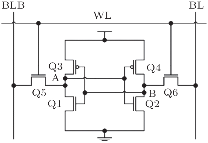
The functional failure mode of HM62V8100I is a temporary function interruption caused by the radiation-induced larger standby current, and the mechanism of temporary function interruption is relevant to peripheral circuits sensitive to standby current rising. Even though the functionality of the device is lost at a dose level of 300 krad, a memory cell array can still be written and read correctly because the device passes the test pattern first tested upon power on. The memory cell of the device is a mainstream six-transistor (6T) CMOS SRAM cell as shown in Fig. 2, four transistors (Q1– Q4) constitute cross-coupled CMOS inverters, and two NMOSFETs Q5 and Q6 provide the read and write access to the cell. For deep sub-micron SRAM, the ultra-thin gate oxide of the memory cell transistor is not affected by total dose irradiation, where the oxide traps generated during irradiation are eliminated by tunnel annealing.[13] But the STI oxide used to isolate transistors still has a thickness of several 100 nm, which is expected to be very sensitive to radiation. The charge trapping in the STI oxide results in excessive leakage current by inverting the channels of the parasitic transistors in NMOSFET.[14] Moreover, because minimum or nearly minimum-geometry transistors are commonly used in SRAM cells, charge trapping in STI oxide also leads to a threshold shift in memory cell transistors, which is well known as the “ radiation-induced narrow channel effect” (RINCE).[15] The functionality of the memory cell will be affected by a radiation-induced threshold shift and off-state leakage current in memory cell transistors. However, experimental results show that functionality of the memory cell array is naturally tolerant to irradiation. In the following, we explore why the functionality of the memory cell array is immune to irradiation by including radiation-induced threshold shift and off-state leakage current in memory cell transistors’ SPICE model.
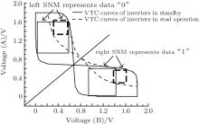
A common metric to characterize the functionality of the memory cell is the static noise margin (SNM) defined as the minimum DC noise voltage necessary to flip the state of a cell. An estimate of the SNM can be obtained by drawing the static voltage transfer characteristic (VTC) curve as illustrated in Fig. 3 and finding the maximum possible square between them. Its side length represents the minimum noise voltage present at each of the cell storage nodes necessary to flip the state of the cell.[16] The functionality of the memory cell is determined by the value of SNM: if both sides’ SNMs of the memory cell are larger than zero, the memory cell can store data “ 0” and “ 1” correctly, while the stuck-at faults take place on the memory cell if one side of SNM decreases to zero. As shown in Fig. 3, the cell is the most vulnerable to noise during a read access, since the “ 0” storage node rises to a voltage higher than ground due to the bit-line discharge, so we should analyze the influence of radiation on functionality of the memory cell through the changing of SNM in the read operation with irradiation (for convenience, the following SNM represents the SNM in read operation).
Fig. 3. Static noise margin definition in memory cell during standby and read operation.
Owing to the process variations in memory cell transistors, different cells have different SNM values in memory cell array and the value of the left SNM is not equal to that of the right SNM in one cell, so that the most sensitive memory cell to irradiation should be considered.[17] The major source of transistor variations is the threshold variation due to the fluctuation in a small number of dopant atoms in the channel.[18] These atomic-level intrinsic fluctuations cannot be eliminated by external control of the fabrication process and are most pronounced in minimum-geometry transistors commonly used in area-constrained circuits such as SRAM cells. The threshold of the transistor satisfies a Gaussian distribution and the standard deviation increases according to CMOS scaling. From International Technology Roadmap for Semiconductors (ITRS) Roadmap, the standard deviation of the threshold for a minimum area transistor of the 0.18-μ m process is 23 mV.[17] Listed in Table 4 are the distribution functions of threshold and W/L ratios of memory cell transistors used in our simulation, with the standard deviation of the threshold selected to be 23 mV. As reported in Ref. [17], the SNM of the memory cell array also satisfies a Gaussian distribution, and the mean value and standard deviation of the distribution can be calculated by a Monte Carlo simulation with the threshold variation parameters listed in Table 4. Determined by a 1000-samples Monte Carlo run, the mean value of SNM is 282 mV and the standard deviation is 2.83 mV. In general, a six-sigma (6σ ) yield or larger is required for large SRAM arrays to be functional, therefore a memory cell with an SNM smaller than mean value 6σ should be considered at least. The SNM of the memory cell that is the value σ of the threshold of transistor deviating from the mean value (Q1, Q4, and Q6 each have a negative deviation of 23 mV, Q2, Q3, and Q5 each have a positive deviation 23 mV) is calculated. The calculation shows that the right SNM is 312.41 mV and the left SNM is 251.55 mV. It is conservative to choose the above memory cell as the most sensitive memory cell to irradiation because the left SNM is 30 mV smaller than the mean value, and is larger than 10σ .
Table 4.
Table 4.
Table 4. SRAM cell transistor sizes and distribution functions of threshold.
Transistor type
W/L ratio
Distribution function of threshold
pull-up PMOSFET
0.22 μ m/0.18 μ m
GAUSS(0.4639236, 0.023)
pull-down NMOSFET
0.35 μ m/0.18 μ m
GAUSS(0.4736658, 0.023)
access NMOSFET
0.22 μ m/0.18‘ μ m
GAUSS(0.4736658, 0.023)
Table 4. SRAM cell transistor sizes and distribution functions of threshold.
The primary cause for radiation-induced off-state leakage current in NMOSFET is the reduction in the threshold and the increase in drive current for the parasitic transistor associated with the edges of the main device. This effect can be modeled as an additional NMOSFET in parallel with the main transistor. By choosing the threshold, the thickness of the gate oxide, and the width of parasitic NMOSFET we can obtain different off-state leakage currents in the main transistor.[19]
Through the above irradiated NMOSFET model, we explore the influence of radiation-induced off-state leakage current in pull down NMOSFET on memory cell SNM. Radiation-induced off-state leakage current in access NMOSFET is not considered in simulation because it is in the state of bias ON during read operation and radiation-induced off-state leakage current is far less than ON current. It can be seen in Fig. 4 that the asymmetry of the memory cell caused by threshold variations of memory cell transistors is enlarged by radiation-induced off-state leakage current in Q1, the left SNM is descending and the right SNM is ascending, but radiation-induced off-state leakage current in Q2 has an inverse influence on SNM compared with that of Q1. From Fig. 5 it follows that the high output level of the inverter composed of Q1 and Q3 is pulled down by the radiation induced off-state leakage current in Q1, resulting in an enlargement of the asymmetry of the memory cell. The off-state leakage current of the pull down NMOSFET increases with irradiation, and the pull up PMOSFET needs to compensate for those leakage currents by lowering down the high output level of the inverter.
Fig. 5. Memory cell SNMs derived by simulation when radiation-induced off-state current in Q1 is 10 μ A. The side length of black square, dashed black square represent pre-irradiation and post-irradiation SNM respectively.
Because the left SNM with a smaller value is reduced by the radiation-induced off-state current in Q1 and the radiation has a larger effect on the ON bias NMOSFET, we assume memory cell store data “ 1” during radiation (Q1 and Q4 are in the state of bias ON, and Q2 and Q3 are in the state of bias OFF), which most likely leads to functional failure in the memory cell. As is well known, standby current of the CMOS device is composed of off-state currents of transistors and the number of SRAM peripheral circuit transistors is far less than that in the memory cell in SRAM, hence the standby current of SRAM mainly comes from memory cell transistors’ off-state leakage currents. Moreover, the increase of standby current only originates from radiation-induced off-state current in Q1 when data “ 0” is stored in memory cells, because radiation does not induce off-state leakage current in PMOSFET. Based on the above analysis, we could obtain the average value of the off-state leakage current of Q1 via dividing the standby current of devices loading inverse data pattern with irradiation by the number of memory cells. The off-state leakage current of Q1 obtained by the above method is larger than its true value because standby current contributed by transistors of the peripheral circuit is added in memory cells. After 300-krad dose of irradiation, the off-state leakage current of Q1 for HM62V8100I is increased to 0.62 nA that has a negligible influence on the memory cell’ s SNM.
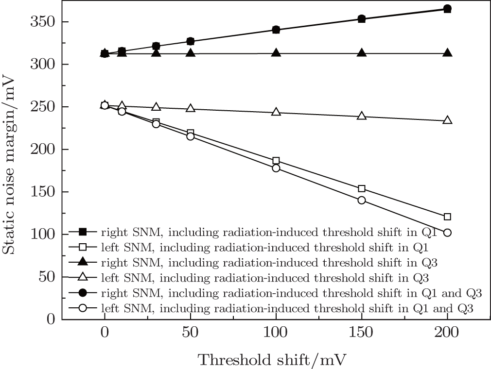
Radiation will cause a negative threshold shift in NMOSFET of the memory cell and a positive threshold shift in PMOSFET due to RINCE. Meanwhile, the effect of radiation is larger at ON bias for NMOSFET in contrast to OFF bias for PMOSFET. The influence of radiation-induced threshold shift on SNM is analyzed by altering the threshold of the transistor in the SPICE model. As shown in Fig. 6, radiation-induced threshold shifts in Q1 and Q3 are considered. Simulation results reveal that the asymmetry of the memory cell is enlarged by the radiation-induced threshold shift and the effects of Q1 and Q3 can be superposed. Furthermore, the threshold shift of PMOSFET has less effect on SNM than that of NMOSFET, and both sides of SNM are still larger than 0 mV when the threshold shift in Q1 and Q3 achieves 200 mV.
Fig. 6. Variations trends of memory cell’ s SNM with radiation-induced threshold shift for Q1 and Q3.
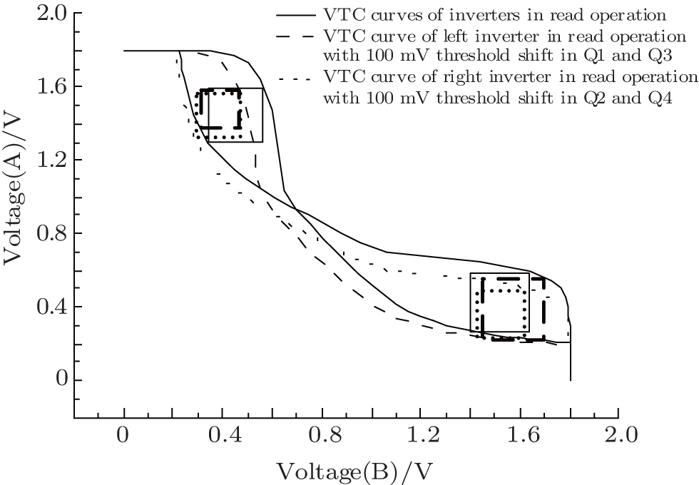
From Fig. 7 it follows that the switch threshold of the inverter is shifted negatively by the radiation-induced threshold shift in Q1 and Q3, leading to degradation in the left SNM, and the influence of radiation-induced threshold shift in Q2 and Q4 on SNM is counter to that in Q1 and Q3.
Fig. 7. Memory cell SNM derived by simulation when radiation-induced threshold shifts in pull up PMOSFET and pull down NMOSFET are 100 mV. The side lengths of the black square and the dashed black square represent pre-irradiation and post-irradiation SNM respectively, while the side length of the dotted black square represents SNM only including radiation-induced threshold shift in Q1 and Q3.
The switch threshold of the inverter is determined by the following equation:
where r is less than 1 due to the smaller width of PMOSFET, so the threshold shift of PMOSFET has less influence on SNM than NMOSFET.
It is conservative to only consider the radiation-induced threshold shift in Q1 and Q3 for determining whether the radiation-induced threshold shift in memory cell transistors results in functional failure. The reasons for this are twofold: 1) owing to the bias effect mentioned above, there is negligible threshold shift in access transistors biased OFF during radiation, 2) the influence of radiation-induced threshold shift in Q2 and Q4 on SNM is counter to that in Q1 and Q3.
Although we cannot measure the thresholds of the memory cell transistor in commercial SRAM before and after radiation, we can obtain the range of threshold shift for a minimum-geometry transistor from the papers on RINCE. Federico Faccio and Giovanni Cervelli studied RINCE in deep sub-micron CMOS transistors.[15] The experimental results showed that the threshold of NMOSFET first decreases and then increases by irradiation behaving as a rebound effect, and the maximum negative threshold shift is 150 mV after 136-Mrad irradiation. Because the build-up of positive trapped charge is fast and the formation of interface states is a slower process in NMOSFET, the negative charge trapped in the interface state only starts to compete with the oxide-trapped charge with some delay, giving rise to a rebound effect. Meanwhile, the threshold shift of PMOSFET is monotonically positive with irradiation due to the charges trapped in the interface states being also positive, which reaches 90 mV at a dose level of 136 Mrad. The above experimental results and theoretical analyses indicate that a radiation-induced threshold shift in the minimum-geometry deep sub-micron transistor is less than 200 mV, which cannot induce functional failure in a memory cell.
By including the radiation-induced threshold shift and off-state leakage current in the memory cell transistor, we analyze the influence of radiation on the functionality of a memory cell. Simulation results reveal that the memory cell is tolerant to irradiation due to its high stability. Despite radiation-induced off-state leakage current in pull down NMOSFET having a negligible influence on the functionality of the memory cell, the standby current of the device will be drastically increased by that leakage current, finally leading to functional failure in the device. When functional failure is detected, the standby current of HM62V8100I is increased to 5.43 mA, 217 times the maximum standby current rating 25 μ A ensured by the datasheet. In order to detect the functional failure of the device correctly, a functional test should be made after the inverse data patterns with irradiation have been loaded into the device. Functional failure of HM62V8100I is detected at a dose level of 120 krad by the functional test after the inverse data pattern with irradiation has been loaded into the device. The mechanism of functional failure for HM62V8100I is relevant to peripheral circuits sensitive to the standby current rising, but we cannot model the total dose response of the peripheral circuit without detailed circuit schematics. Furthermore, devices from different vendors have different circuit schematics, then exhibit complex functional failure modes depending on different circuit schematics. Functional failure modes of commercial SRAMs are hard to predict due to the unknown peripheral circuit schematics, which is a challenge to using the commercial SRAMs in a total dose radiation environment safely.
5.Conclusions
Functional failure mode of the commercial deep sub-micron SRAM is studied in our paper. Experimental and theoretical results indicate that the memory cell of the deep sub-micron SRAM is naturally tolerant to irradiation due to its high stability, and functional failure of the device is caused by peripheral circuits sensitive to standby current rising behaving as a temporary function interruption. Though radiation-induced off-state in pull down NMOSFET has a negligible influence on the functionality of the memory cell, the standby current of the device will be drastically increased by that leakage current, finally triggering functional failure in the device. In order to detect the functional failure of the device correctly, functional testing should be made on condition that devices have the maximum standby current.
JonathanPellish2012Nuclear and Space Radiation Effects Conference Short Course NotebookMiami: IEEESection II[Cited within:1]
5
ASTM F1892-12 Stand ard Guide for Ionizing Radiation ( Total Dose) Effects Testing of Semiconductor DevicesDOI:10.1520/F1892-12[Cited within:1]
6
LaBelKenneth A, GigliutoRobert A, SzaboCarl MJr, CartsMartin A, KayMatthew, SinclairTimothy, GadlageMatthew, DuncanAdam and IngallsDave2013Radiation Effects Data Workshop (REDW)July 8–12San Francisco, CA, USA1DOI:10.1109/REDW.2013.66581982013[Cited within:1]
7
JhaN K and GuptaS2003Testing of Digital SystemsNew YorkCambridge University Press845[Cited within:2]
8
DoucinB, PoiveyC, CarlottiC, SalminenA, OjasaloK, AhonenR, PoirotP, BaudryL and SorensenR H1997Fourth European Conference on Radiation and Its Effects on Components and Systems, 1997 RADECS 97September 15–19, 1997Cannes561DOI:10.1109/RADECS.1997.6990011997[Cited within:1]
LelisAivars J, MurrillSteven R, OldhamTimothy R and RobertsonDale N1996IEEE Trans. Nucl. Sci. 431535DOI:10.1109/23.556911[Cited within:1]
11
HashG L, ShaneyfeltM R, SextonF W and WinokurP S1997Radiation Effects Data Workshop, 1997 IEEEJuly 24, 1997Snowmass Village, CO35[Cited within:1]
12
KimVonkyoung and ChenTom199715th IEEE VLSI Test Symposium, 1997April 27–May 1, 1997Monterey, CA, USA24DOI:10.1109/VTEST.1997.5994371997[Cited within:1]
... [1] Unfortunately, radiation hardness assurance of COTS components can be extremely challenging since most commercial manufacturers have no motivation to identify and monitor the technology parameters that affect the radiation hardness of their products ...
2
2006
0.0
0.0
... [2] As is well known, total dose irradiation in insulating material results in cumulative parametric degradation in electronics and finally leads to functional failure, so we need to perform functional testing to ensure their functionalities in hardness assurance testing ...
... [2] Functional testing after anneal shows that the functional failure of the device is triggered by the inverse data pattern with irradiation where the device has the maximum standby current, indicating that the larger standby current caused by irradiation is responsible for the functional failure of the device ...
1
2013
0.0
0.0
... [3,4] Functional testing for electronics requires the application of test vectors to inputs and monitoring the output for correct results, and test vectors are designed based on functional failure modes of devices ...
1
2012
0.0
0.0
... [3,4] Functional testing for electronics requires the application of test vectors to inputs and monitoring the output for correct results, and test vectors are designed based on functional failure modes of devices ...
1
0.0
0.0
... [5] However, it is difficult to identify functional failure modes of COTS advanced electronics induced by radiation, because the more advanced functions and detailed information are trapped at a die level, and COTS devices are #cod#x201C ...
1
2013
0.0
0.0
... [6] ...
2
2003
0.0
0.0
... [7] Functional test patterns are designed based on the characteristics of the above functional failure modes, and the most used functional test patterns in total dose hardness assurance testing of SRAM are Solid and Checkerboard designed for stuck-at faults (test vectors running to memory are called test patterns) ...
... [7] At the same time, DC and AC electrical parameters of devices are also measured ...
1
1997
0.0
0.0
... [8#cod#x2013 ...
1
2002
0.0
0.0
1
1996
0.0
0.0
1
1997
0.0
0.0
... 11] But to the best of our knowledge, there is no study that demonstrates that the functional failure modes of SRAM induced by irradiation are stuck-at faults, so that the hardness of the device may be overestimated by the Solid and Checkerboard ...
1
1997
0.0
0.0
... [12] However, the mechanism of functional failure induced by irradiation is different from physical defects, which result in a break or bridge in one node of the circuit, leading to functional failure, while functional failure induced by irradiation is due to the changes of electrical characteristics of transistors ...
1
2003
0.0
0.0
... [13] But the STI oxide used to isolate transistors still has a thickness of several 100#cod#x00A0 ...
1
2011
0.0
0.0
... [14] Moreover, because minimum or nearly minimum-geometry transistors are commonly used in SRAM cells, charge trapping in STI oxide also leads to a threshold shift in memory cell transistors, which is well known as the #cod#x201C ...
2
2005
0.0
0.0
... [15] The functionality of the memory cell will be affected by a radiation-induced threshold shift and off-state leakage current in memory cell transistors ...
... [15] The experimental results showed that the threshold of NMOSFET first decreases and then increases by irradiation behaving as a rebound effect, and the maximum negative threshold shift is 150#cod#x00A0 ...
1
2005
0.0
0.0
... [16] The functionality of the memory cell is determined by the value of SNM: if both sides#cod#x2019 ...
3
2001
0.0
0.0
... [17] The major source of transistor variations is the threshold variation due to the fluctuation in a small number of dopant atoms in the channel ...
... [17] Listed in Table#cod#x00A0 ...
... [17], the SNM of the memory cell array also satisfies a Gaussian distribution, and the mean value and standard deviation of the distribution can be calculated by a Monte Carlo simulation with the threshold variation parameters listed in Table#cod#x00A0 ...
1
1998
0.0
0.0
... [18] These atomic-level intrinsic fluctuations cannot be eliminated by external control of the fabrication process and are most pronounced in minimum-geometry transistors commonly used in area-constrained circuits such as SRAM cells ...
1
2005
0.0
0.0
... [19] ...
Analysis of functional failure mode of commercial deep sub-micron SRAM induced by total dose irradiation
[Zheng Qi-Wena),b),c), Cui Jiang-Wei†a),b), Zhou Hanga),b),c), Yu De-Zhaoa),b),c), Yu Xue-Fenga),b), Lu Wua),b), Guo Qia),b), Ren Di-Yuana),b)]


 , Zhou Hang