


Analysis of the spatial filter of a dielectric multilayer film reflective cutoff filter-combination device
[Zhang Yinga), b) , Qi Hong-Jia) , Yi Kuia) , Wang Yan-Zhia) , Sui Zhanc) , Shao Jian-Da†a)  ]
]
]
|
|


†Corresponding author. E-mail: jdshao@siom.ac.cn
The experiment setup of a reflecting combination device, which has more advantages than a transmitting combination device, is designed in this study. To achieve angular spectrum selectivity, only one type of reflective component is needed, so difficulties of design and preparation are reduced. A dielectric multilayer film is applied to the reflective component, and the long wave-pass coating stacks of the structure are designed. To achieve high stopband transmittance and reduce electric field intensity at a wavelength of 1053 nm, an objective function is proposed for designing an optimized coating. The final optimized coating has good spectral characteristics and a high laser-induced damage threshold. A dielectric multilayer film with high reflectance plays an important role in preparing and applying a dielectric multilayer film reflecting cutoff filter-combination device.
As an important device in large, complex, high-power laser systems, a spatial filter can be used to remove components with high angular frequency, thus reducing the output of laser light-modulated small-scale intensity distribution and improving the quality of a laser beam.[1– 13] Spatial filters can be classified as two categories, depending on whether the beam must be focused, namely, the focusing method and the non-focusing method. The most typical structure in the focusing method is the pin-hole filter, which is widely used in available laser systems.[14, 15] Although the pin-hole spatial filter is widely used for beam cleanup, [3, 4, 9] its required focusing of the laser beam presents poor functionality, especially in high-power laser fields. For example, the induced plasma may approach to the pin-hole, deflect the laser beam into the incident system, and probably damage the optical devices in the system because of the high power density close to the pin-hole.[16– 18] A new design concept is necessary to reduce the size of the laser filter system, thus replacing the traditional large-size spatial filter in a high-power laser system.
In this study, we propose the use of a reflective combination device to realize the spatial filtering function in a high-power laser system. The reflective combination device can spatially filter the deformed laser beam directly without any focusing, so the previously mentioned pin-hole filter drawbacks are avoided.[13] The reflective combination device also occupies much less volume and weight than the pin-hole filter. Thus, the device can be used in air and space environments. Compared with a transmittance combination device, a reflective combination device only uses two identical reflective components to achieve a spatial filter, so difficulties of design and preparation are considerably reduced. Finally, a dielectric multilayer film is applied in the reflective component. The long wave-pass coating stacks of the structure are designed. To achieve good spectral characteristics of the coating, the optimized design is presented, but the electric field intensity at a wavelength of 1053 nm is increased. An objective function is therefore proposed to design an optimized coating, thus achieving high stopband transmittance and reducing electric field intensity. Doing so can maintain the lower electric field intensity of the coating and effectively improve the laser-induced damage threshold. The reduced electric field intensity of the coating is effective in the application field of the filter. As a result, the combination of cutoff filters may be put into practical applications of laser system devices.
Although the potential of a reflective component to spatially filter laser beams has been theoretically analyzed in the past, few studies have presented an experimental analysis of the beam cleanup capability of such a component. An experiment is therefore designed in this study to verify the spatial filtering performance of a reflective component for spatially deformed laser beams.
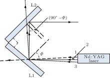
The schematic diagram of the experimental setup for the reflective cutoff filter-combination device reflectivity is shown in Fig. 1. The optical components along the incident beam from the Nd:YAG laser are sequentially reflective components L1, L2; L1, L2 are placed vertically; and L1 is placed opposite L2. Here, Φ is the incidence angle and is generally defined as 45° . The laser beams 1, 2, and 3 represent light incident at angles less than, equal to, and greater than 45° , respectively. Only the incidence angle that is equal to or greater than those in the cases of incident laser beams 2 and 3 can be reflected from L1 to L2. When light beam 3 is incident on L2, the incidence angle becomes (90° − Φ ) because of the complementarity. The beam whose original incidence angle is less than 45° will also be filtered by L2. Finally, the beam with an original incidence angle of 45° is reflected by L2, so angular spectrum selectivity is achieved. The design of reflective combination device spatial filters suggests that this structure can play a role in determining angular spectrum selectivity at an oblique incidence angle of 45° . Reflecting cutoff filter-combination devices have complementary angle characteristics and can reduce component requirements compared with transmission combination devices, [19] and the two identical components may achieve the selectivity of the angular spectrum. In general, the incidence angle is set to be 45° . Compared with a transmission combination device, the reflective combination device has an angular spectrum selectivity that can be achieved by using only one component. As such, difficulties of design and fabrication are considerably reduced.
 | Fig. 1. Schematic diagram of the experimental setup for the cutoff filter-combination device (L1, L2: reflective component). |
Reflective components L1 and L2 must have high reflectance and high transmittance to make the spatial filter in the experiment setup reflect the cutoff filter-combination device. Therefore, a dielectric multilayer film, which has properties of high reflectance and high transmittance, is used to effectively achieve the selectivity of the angular spectrum. The film has angle sensitivity, and the phase shift can also drift; as the incidence angle increases, the spectrum drifts toward shortwave and vice versa.[20] Although the multi-layer dielectric film theoretically has the potential to spatially filter the laser beam, few studies have presented an experimental analysis of the beam cleanup ability of the film. The dielectric multilayer film is therefore one of the most promising reflective components in a combination device.
Nb2O5(2.20@1053 nm), Ta2O5(2.04@1053 nm), HfO2(1.92@1053 nm), and Al2O3(1.61@1053 nm) are usually high index materials, whereas SiO2(1.45@1053 nm) is a low refractive index material. A wide bandwidth and a steep transition edge are needed because of the high reflection and high transmission, and the higher refractive index material is beneficial to the same layer thickness. On the other hand, a long wave-pass film is less thick than a short wave-pass, so a long wave-pass film made of a high refractive index material, such as Ta2O5, and a low refractive index material, such as SiO2, is used to design the dielectric multilayer film reflective component. As a result, high reflectance at 1053 nm and high transmittance at 1057 nm can be achieved.
The width of the zone should be close to 4 nm, and steep reflectance slope should exist between the reflectance and rejection zones. The target reflectances for this filter are 99% at 1053 nm and 1% at 1057 nm respectively. Compared with the P-polarized wave, the S-polarized wave can improve angle sensitivity in oblique incidence, so the S-polarized component is selected.
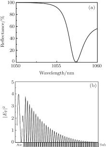
The initial design of the reflectance of the long wave-pass reflecting film in its basic structure is as follows: Sub| (0.5HL0.5H)38| Air. “ Sub” denotes substrate, and “ Air” denotes air. The substrate has a refractive index of 1.52. “ H” denotes an optical thickness of one-quarter wavelength at a wavelength of 1053 nm with the Ta2O5 (2.04@1053 nm) layer, and “ L” denotes that with the SiO2 (1.45@1053 nm) layer. The reflectance spectral curve of the long wave-pass reflecting cutoff filter at an incidence angle of 45° is shown in Fig. 2(a). The electric field distribution of the long wave-pass reflecting cutoff filter-combination device at an oblique angle of incidence of 45° is shown in Fig. 2(b). The maximum value of the normally incident electric field is 3.5.
 | Fig. 2. Initial design of the long wave-pass reflecting cutoff filter at an incidence angle of 45° , showing (a) reflectance spectral curve and (b) electric field distribution at a wavelength of 1053 nm. |
The reflectance spectral curve shows that the long wave-pass reflecting cutoff filter has many side lobes, and the max of the transmittance is only 90%. Therefore, the thickness values of the several front and back layers are optimized to improve the transmittance of the passband region. The optimized design of the reflective films in the basic structure is as follows: Sub| .0748H1.139L1.0301H1.2837L(0.5HL0.5H)38 1.8181L0.6216H0.8832L1.0217H| Air.
The reflectance spectral curve of the long wave-pass reflecting cutoff filter at an incidence angle of 45° is shown in Fig. 3(a), in which the side lobes are effectively suppressed, and the high stopband reflectances are maintained. The transmittances over 1059 nm– 1063 nm are all greater than 99%. The electric field distribution of the long wave-pass reflecting cutoff filter-combination device at an oblique angle of incidence of 45° is shown in Fig. 3(b). The maximum value of the incident normalized electric field is 6. The electric field intensity of the optimized design increases compared with that of the initial design, and the laser damage threshold in high-power laser films decreases.
 | Fig. 3. Optimized design of the long wave-pass reflecting cutoff filter at an incidence angle of 45° , showing (a) reflectance spectral curve and (b) electric field distribution at a wavelength of 1053 nm. |
To achieve high stopband transmittance and reduce electric field intensity at a wavelength of 1053 nm, the process for designing a final optimized coating is outlined below. The objective function here is to maximize reflectivity R and minimize electric field intensity E at a single wavelength of λ = 1053 nm:

where MF is the objective function, WE and WR are the weight factors:

The final optimized design of the basic structure of the long wave-pass reflecting cutoff filter is as follows:

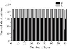
The layer thickness structures of the final design are shown in Fig. 4. The corresponding structure consists of 80 alternating layers of Ta2O5, which has a high refractive index, and SiO2, which has a low refractive index. The physical layer thickness is 12.1 μ m.
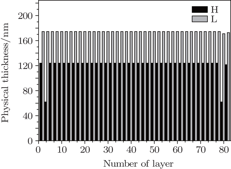 | Fig. 4. Physical thickness of the layer versus layer number for the final optimally designed reflective film, where H represents the highly refractive material Ta2O5 and L refers to the lowly refractive material SiO2. |
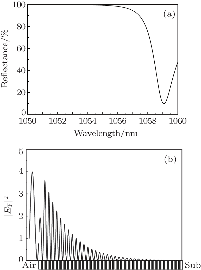
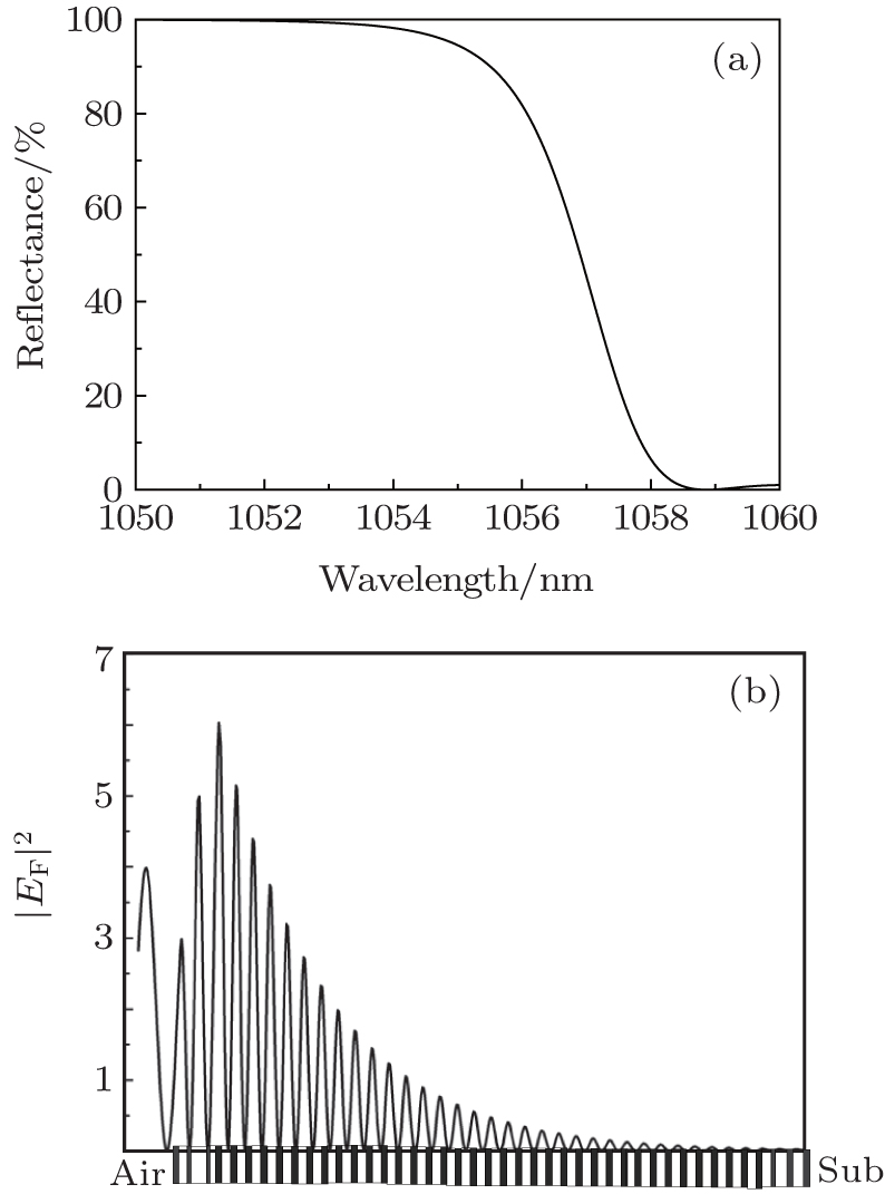
For a final optimally designed filter, the reflectance spectral curve in a long wave-pass reflecting cutoff filter at an incidence angle of 45° is shown in Fig. 5(a), in which the max value of transmittance is up to 99.5%. The electric field distribution at a wavelength of 1053 nm is shown in Fig. 5(b), in which the maximum value of the incident normalized electric field is 3.5. By comparison, the present device has an electric field intensity almost the same as that of the initial device, and it also has a laser damage threshold of the film that is higher than that of the initial device. Therefore, the present design is considered to be optimal.
 | Fig. 5. Final optimal design of the long wave-pass reflecting cutoff filter at an incidence angle of 45° , showing (a) reflectance spectral curve and (b) electric field distribution at a wavelength of 1053 nm. |
Figure 6 shows the variation of reflection with angle of the long wave-pass cutoff filter-combination device with an oblique angle of incidence of 45° at a central wavelength of 1053 nm. The angular sensitivity is defined as the full-width at half maximum (FWHM) of the angular spectrum. The FWHM of the angular spectrum is 1.8° .
 | Fig. 6. Reflectance of the long wave-pass reflecting cutoff filter-combination device versus angle. |
In this paper, we propose the use of a reflective combined device to achieve spatial filtering of a laser beam. We design an experiment setup, which consists of two perpendicular reflective components to filter the incident light in mutually orthogonal directions, thus realizing the entire optical path of the incident beam spatial filtering function. Compared with a transmitting cutoff filter-combination device, the present device not only reduces the reflection to half that of the component type but also lessens the difficulty of preparation. We also propose the use of reflective components to achieve a multilayer dielectric film, and we design the long wave-pass coating stacks of the reflecting film. When the optimized design is utilized in the initial coating stacks, the side lobes of the spectra decrease, and the transmittance of the passband region is also improved. However, the electric field intensity increases. The objective function is proposed to design an optimal coating, thus achieving high stopband transmittance, reducing the electric field intensity, and enhancing the final optimized design of the long wave-pass reflecting cutoff filter. The reflecting component of the multilayer dielectric film has a low electric field and is suitable for applications in high-power laser systems because of the high laser-induced damage threshold of the film. Therefore, the use of combined device filters is a promising method to replace the use of large-size spatial filters in high-power laser systems. These filters have practical applications as well.
| 1 |
|
| 2 |
|
| 3 |
|
| 4 |
|
| 5 |
|
| 6 | [Cited within:1] |
| 7 |
|
| 8 |
|
| 9 |
|
| 10 |
|
| 11 |
|
| 12 |
|
| 13 |
|
| 14 |
|
| 15 |
|
| 16 |
|
| 17 |
|
| 18 |
|
| 19 |
|
| 20 |
|