


Confinement-induced nanocrystal alignment of conjugated polymer by the soft-stamped nanoimprint lithography
[Li Xiao-Huia) , Yu Ji-Chengb) , Lu Nai-Yana) , Zhang Wei-Donga) , Weng Yu-Yan†a)  , Gu Zhen‡
b) ]
, Gu Zhen‡]
|
|


†Corresponding author. E-mail: wengyuyan@suda.edu.cn
‡Corresponding author. E-mail: zgu@email.unc.edu
*Project supported by the National Natural Science Foundation of China (Grant No. 21204058).
Soft-stamped nanoimprint lithography (NIL) is considered as one of the most effective processes of nanoscale patterning because of its low cost and high throughput. In this work, this method is used to emboss the poly (9, 9-dioctylfluorene) film. By reducing the linewidth of the nanogratings on the stamp, the orientations of nanocrystals are confined along the grating vector in the nanoimprint process, where the confinement linewidth is comparable to the geometrical size of the nanocrystal. When the linewidth is about 400 nm, the poly (9, 9-dioctylfluorene) (PFO) nanocrystals could be orderly arranged in the nanogratings, so that both pattern transfer and well-aligned nanocrystal arrangement could be achieved in a single step by the soft-stamped NIL. The relevant mechanism of the nanocrystalline alignment in these nanogratings is fully discussed. The modulation of nanocrystal alignment is of benefit to the charge mobilities and other performances of PFO-based devices for the future applications.
In the past decades, conjugated polymers have received great attention as the cost-effective function materials in organic semiconductor area.[1] The performances of the conjugated polymer-based devices are affected by both polymer morphology and the nanocrystals alignment.[2– 4] As one of the most interesting blue-emitting conjugated polymers, poly (9, 9-dioctylfluorene) (PFO) has attracted more and more attention for use in light-emitting diodes and field-effect transistors.[5, 6] Therefore, it is crucial to modulate the nanocrystal alignment[7] to improve the performances of PFO device. Previous studies suggested that the chain or orientation of nanocrystal could be modulated by drying process and surface modulation.[8] Under the consideration of physical and chemical stability, [3] nanoimprint lithography (NIL) has been developed by providing a high-resolution lithography through replicating the nanostructures from hard molds.[3, 9– 12] We previously demonstrated that hard-stamped NIL could induce molecular orientation and directly achieve the desired nanostructures in conjugated polymer thin film.[10] Of note: we found that the preferential nanoimprinting-induced molecular orientation had a great influence on the performances of ferroelectric polymers and photoactive azobenzene liquid crystalline elastomers (LCEs).[11, 12] We believed that the NIL process is the most optimal technique to achieve the complete spatial design and nanocrystals alignment of the PFO film.
Although the hard-stamped NIL seemed to be the best candidate for nanostructure fabrication of the macromolecular materials, the cost of hard stamp fabrication was still extremely high. In order to reduce the cost of the template fabrication, it is significant to develop a simply soft-stamped NIL for the pattern transfer fidelity and the orientation modulation of nanocrystals.[13, 14] In addition, the comprehensive understanding of the alignment of nanocrystals under the soft-stamp-defined confinement is still unknown. Herein NIL with the soft stamp polydimethylsiloxane (PDMS) directly replicated from the polymethyl methacrylate (PMMA) nanogratings is used to discuss the influencing factors of the orientation degree of PFO nanocrystals. Both the x-ray diffraction and the cross extinction image are used to analyze the orientation degree of nanocrystals. To have a better understanding of the nanocrystals alignment in soft-stamp-defined confinement, the relevant mechanism is also discussed.
The PMMA photoresist template was directly achieved by the electron beam lithography (EBL) as a mother template. First, the photoresist PMMA (AR-P 671, PMMA photoresist, Allresist, Germany) was spin-coated at 2000 rpm on the carefully cleaned silicon wafer about 1 min. Second, the PMMA film was baked on a hot plate at 180 ° C for about 5 min. Finally, following the preset program, the designed pattern was acquired under the focused electron beam and presented after the developer and the stopper.
To minimize the cost of the template fabrication, the self-crosslinking and anti-adhesive properties of PDMS were fully used. The PDMS (SLYGARD 184, Dow Corning, USA) was used as soft stamp material here to duplicate the pattern from the PMMA mother template. First, the PDMS base and its curing agent were mixed sufficiently at a ratio of 10:1. Second, the PDMS mixture was dropped on that mother template. As the surface energy difference between PMMA and PDMS, the embossed PDMS film was easily striped off after its self-crosslinking. So that the soft stamp PDMS was obtained in this way, the detailed experiment condition could be found in Ref. [14].
The PFO (ADS129BE, American Dye Source) was dissolved in toluene with a concentration of 15 mg/ml. The solution was dropped on the silicon wafer and spincoated at 4000 rpm to obtain the 60-nm-thick PFO film. The PFO film was achieved by thermal annealing at 180 ° C for 5 min, then 135 ° C for 10 min and cooling to room temperature. The PDMS stamp was put against the PFO film. Then, the PDMS stamp was pressed against the PFO film by using a nano-imprinter (Obducat, Eitre 3) under the pressure 40 bar (1 bar = 105 Pa) at 180 ° C for 5 min to make sure that nano-trenches in the mold were completely filled, then cooled to 135 ° C and kept for 10 min, and cooled to the room temperature. The nanoimprinting process was schematically shown in Fig. 1(a).
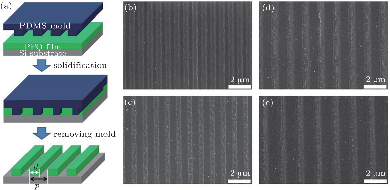 | Fig. 1. Fabrication of array of PFO nanowires. (a) Schematic diagram of the nanoimprint process. (b)– (e) SEM morphologies of nanogratings. |
In order to guarantee that the experiment conditions are equal, the four different linewidth nanogratings were designed on one PDMS soft stamp. On the one hand, the imprinting condition could be the same; on the other hand, the imprinting depth and the residual layer thickness could be equal. Hence, these four different linewidth PFO nanogratings were achieved on one PFO film spontaneously.
The morphological characterizations of PFO nanogratings were carried out with the field emission scanning electron microscope (FESEM, Pioneer, Raith) and the atomic force microscopy (AFM, MFP-3D, Asylum Research) respectively. The arrangement of molecular chains inside the nanogratings was studied by the grazing incidence wide angle x-ray diffraction (GIWAXD, Shanghai Synchrotron Radiation Facility) and the polarized optical microscopy (POM, DM4000, Leica).
The PFO nanogratings are fabricated via a soft-stamped NIL technique (Fig. 1(a)). As shown in Figs. 1(b)– 1(e), the PFO gratings with four different values of linewidth (d) are reproduced on one silicon wafer. These four line-width nanogratings are designed into the same duty cycle (f = d/p) around 0.5 with different periods, and the values of period (p) are 0.8 μ m, 1 μ m, 1.4 μ m, and 1.6 μ m respectively. From the SEM morphology characterization, the PFO nanogratings are duplicated precisely from the PDMS soft stamp.[14] All of the PFO nanogratings are uniform in height and width, and the residual layer thickness should be equal.
The AFM image of 1-μ m period PFO grating is taken for example to show good agreement between the PDMS soft stamp and the PFO nanograting as shown in Fig. 2. Figures 2(a) and 2(b) show AFM images of the PDMS soft stamp and the PFO nanograting and figures 2(c) and 2(d) show the surface profiles of the PDMS soft stamp and the PFO nanograting marked as grey lines in Figs. 2(a) and 2(b). Both the AFM images and the surface profiles demonstrate that the PDMS soft stamps could withstand and imprint the PFO film over Tg under a 40-bar pressure, and the PFO grating is copied precisely from the PDMS soft stamp.
 | Fig. 2. PDMS soft stamp and PFO nanograting of 1-μ m period. (a) The AFM image of PDMS soft stamp. (b) The AFM image of PFO nanograting. (c) The surface profile of PDMS soft stamp marked as the grey line in Fig. 2(a). (d) The surface profile of PFO nanograting marked as the grey line in Fig. 2(b). |
As demonstrated in Ref. [15], the nanocrystalline orientation can be affected by the confinement geometry in hard template NIL system, meanwhile the nucleation process, the crystal growth process, the crystallization process and the confinement itself may affect the final orientation of molecular chains or the nanocrystalline. With the consideration of the bad electrical conductivity and ultrathin film thickness of the PFO nanogratings, the x-ray technique is used to detect the internal nanocrystalline arrangement in these nanogratings, as the GIWAXD is really helpful in detecting the orientation of the polymer materials.[10] The BL14B1 Beamline at the Shanghai Synchrotron Radiation Facility in China was fully supported, whose incident azimuth was fixed about 0.18° to probe the orientation.
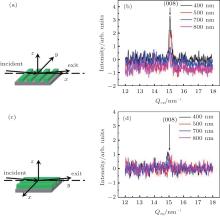
In order to understand the special molecular chain arrangement in these nanogratings, both the longitudinal and cross sections are detected by the grazing incident x-ray in different incident directions Here, we define the diffraction vectors Qxy and Qz pointing along and normal to the substrate plane. The peaks at Q = 15.1 nm− 1 and Q = 4.8 nm− 1 correspond to the plane (008) and (200) of PFO orthorhombic crystal unit respectively.[16] Apparently, the intensity profile can indicate the order degrees of the PFO molecular chain arrangement in these different linewidths nanogratings. As the contrasts of these peaks in the two-dimensional (2D) GIWAXD images of different sections are hard to be quantitative, the one-dimensional (1D) integration results are used here to identify the peak intensities along the diffraction vectors Qxy and Qz.
First, the longitudinal sections of the nanogratings with different linewidths are discussed in Figs. 3(a) and 3(b). Figure 3(a) shows the x-ray path. The GIWAXD image of the x-ray intensity distribution in this section is obtained on the CCD. By the 1D integration of the intensity profile of GIWAXD image along the diffraction vector Qxy, the intensity peak of the reflection of (008) plane is found at 15.1 nm− 1 as shown in Fig. 3(b). These four curves with different colors represent the intensities of profiles along the Qxy in longitudinal sections of nanogratings with four different linewidths. The values of linewidth (d) are 400 nm, 500 nm, 700 nm, and 800 nm respectively. The maximum intensity of the (008) plane appears at a minimum linewidth of about 400 nm, as the peak intensity decreases with the linewidth increasing. The enhancement of the peak intensity may come from the nanocrystalline reorientation under the effective confinement in the NIL process.
 | Fig. 3. Identification of molecular chains alignment by plane (008) in the substrate plane along Qxy. (a) The x-ray path incident in the direction perpendicular to the nanogratings. (b) The 1D integration of GIWAXD intensity along Qxy incident in the direction perpendicular to nanogratings. (c) The x-ray path incident in the direction parallel to the nanogratings. (d) The 1D integration of GIWAXD intensity along Qxy incident in the direction parallel to nanogratings. |
Second, the x-ray intensity distributions in the cross section of these nanogratings are discussed in Figs. 3(c) and 3(d). Figure 3(c) shows the x-ray path and figure 3(d) displays the 1D integration of (008) plane intensity profile of GIWAXD image along the diffraction vector Qxy. Unlike the x-ray distribution in longitudinal section, the peak intensities of the plane (008) almost keep constant in Fig. 3(d). This constant performance of the peak intensity may come from the unchangeable order degree inside the PFO nanocrystalline during the PFO crystallization.
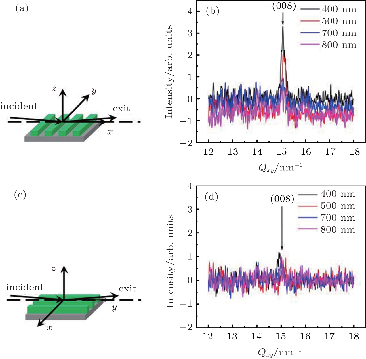
Third, in order to verify the (008) plane intensity distribution in the nanogratings, the (200) plane intensity distributions in 400-nm and 800-nm linewidth nanogratings are checked in Fig. 4. Since these two planes should be perpendicular to each other, the peak intensity distributions should be in consistent with each other. The x-ray paths to identify the longitudinal and cross section are marked in black and red in Fig. 4(a). The 1D integrations of (200) plane intensity profile of GIWAXD image along the Qz are shown in Fig. 4(b). Correspondingly, the (200) plane intensity in 400-nm linewidth nanograting in the longitudinal section is almost twice that in cross section, whereas the intensities in 800-nm linewidth array keep identical in these two sections (Fig. 4(b)). This peak intensity distribution of plane (200) indicates that the molecular chain arrangement along the confinement edge can be realized by shrinking the confinement size in cooperation with the peak intensity distribution of plane (008).
 | Fig. 4. Identification of molecular chain alignment by plane (200) normal to the substrate plane along Qz. (a) The x-ray path incident in the direction perpendicular to (black arrows) and along (red arrows) the nanogratings. (b) The 1D integration of GIWAXD intensity along Qz incident in the direction perpendicular to (black curves) and along (red curves) nanogratings with linewidth 400 nm (curves with empty circles) and 800 nm (smooth curves). |
In orthorhombic crystal unit, the three axes a, b, and c are perpendicular to each other, so are the planes (h00), (0k0), and (00l). In the PFO orthorhombic crystal unit, c axis is usually set to be along the conjugated chain direction in conjugated plane, while b axis is set to be perpendicular to the c axis in the conjugated plane and a axis normal to the conjugated plane. From the previous results, the integration intensity of (008) plane increases with the linewidth shrinking in the longitudinal section of the nanogratings as shown in Fig. 3(b), while the cross section keeps constant as shown in Fig. 3(d), so that the c axis is arranged more regularly in narrower confinement in the longitudinal section, while cross section keeps unchanged. Therefore, the arrangement of polymer molecular chains is influenced greatly along the confinement edge by the confinement scaling, and keep constant in the direction perpendicular to the confinement edge. And the x-ray diffraction distribution of plane (200) in Fig. 4(b) supports our preliminary conclusion that the polymer molecular chains are arranged more regularly under the narrower confinement.
As is well known, the arrangement of macromolecular chains could not be controlled by the submicro scaling confinement, [15] so some other reorientation mechanisms should take place after the PFO nucleation process. Hence, the arrangement of the PFO nanocrystals is investigated by POM. As shown in Fig. 5(a), the sample is in the reflected cross extinction mode under the microscope system. In this mode, the polarization directions of polarizer filter A and analyzer filter B are set to be perpendicular to each other as indicated by the solid arrow and the dotted arrow in Fig. 5(a). So if the sample with linear polarization is rotated in the xy plane, the reflected intensity can be changed with the rotation angle. Here we take the grating vector to be parallel to the nanograting, and set the angle between the grating vector and the polarization direction of polarizer filter A as α , which starts from α = 0° , when the grating vector is parallel to the polarization direction of polarizer filter A. As the sample is rotated in xy plane, α increases from 0° to 90° , and the maximum reflected intensity is taken at α ≈ 45° as shown in the inset of Fig. 5(b), where the PFO grating edge area is chosen to take this POM image. These four grating structure areas are in the middle of the entire PDMS soft stamp, and the remaining areas are all flat. After the NIL, both the flat PDMS and nano-trenched PDMS are pressed against the PFO film, so the flat PFO and PFO nanogratings could appear spontaneously in the entire PFO film. When this PFO grating edge area is observed under the POM system, the flat PFO and the PFO nanograting reflect in different behaviors. The overall intensity of the flat film is low and changeless, while that of the PFO nanograting changes with α as mentioned above. The inset image of Fig. 5(b) is taken at the edge of 400-nm linewidth nanograting area. The bright region at the lower right corner is the embossed PFO nanograting, and the dark one at upper left corner is the flat PFO film. Figure 5(b) shows the variation of the ratio between the maximum intensity and the intensity at 800-nm linewidth nanograting with linewidth. Their maximum intensity increases with linewidth shrinking. For the grating of the homogenous material, the reflected intensity from the grating surface can be calculated precisely, so the difference between the observed and calculated reflected intensity can be easily estimated. This difference may come from the reflected loss under the different linewidths of PFO nanogratings, so this difference gives an indication of the nanocrystal arrangement inside these nanogratings.
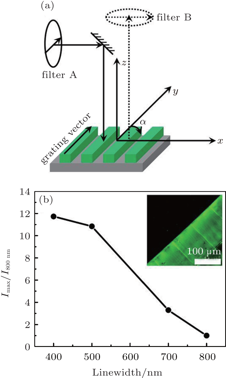 | Fig. 5. Alignment of nanocrystals within the nanowires. (a) The schematic optical path of the reflected cross extinction mode. (b) Relative maximum intensity with different linewidths. |
As the confinement scaling in our imprinting lithography is on the order of around sub-micrometer, this kind of confinement cannot influence the nanocrystal nucleation, but can influence the arrangement of nanocrystals. The PFO films are annealed under the same condition, no matter whether the nanoconfinement exists or not, so the major distribution of the PFO nanocrystals inside nanogratings should be the same as that inside the unembossed PFO film.[10] Hence, the unembossed PFO film in the same annealing condition is analyzed by the optical microscopy as shown in Fig. 6(a), and the inset shows the AFM image. In the reflected microscopic image, the differently oriented nanocrystals are distributed next to each other in the way of alternating light and dark areas, while the AFM image supports this phenomenon. By the careful measurement of nanocrystals in the reflected microscopic image, the length scales of major distribution for each nanocrystal in long and short axes are about 800 nm and 400 nm as indicated in Figs. 6(b) and 6(c).
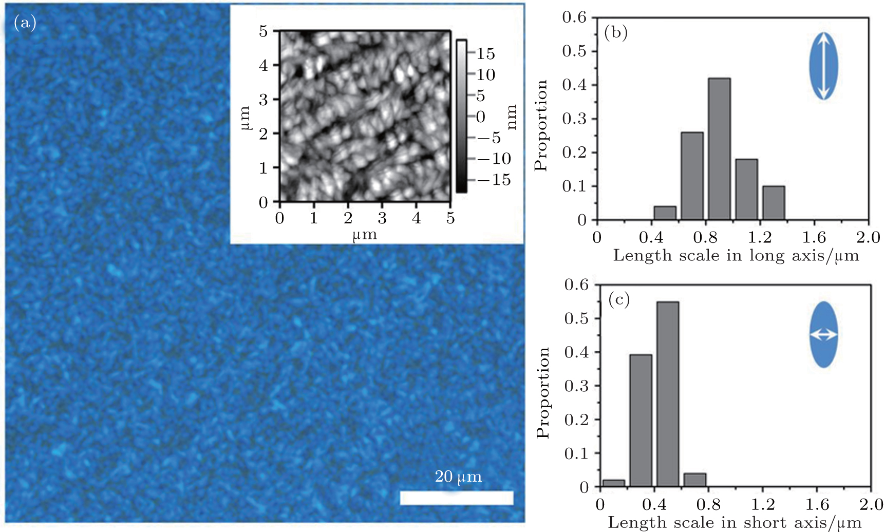 | Fig. 6. Nanocrystal dimension in the film. (a) Microscopic image of the unembossed PFO film in reflected cross extinction with AFM image inserted. (b) and (c) The size distribution of these nanocrystals in PFO film. |
For the lenticular PFO nanocrystals, the backbones are always parallel to its long axis, [17] so the c axis always lays along the long axis with a length scale of about 800 nm under this annealing condition. Once the reorientation process happens under a confinement scale lower than 800 nm, the nanocrystals are less free to choose the orientation direction. As a result, the long axis has a high possibility to be located in the grating vector direction. When the confinement scale becomes smaller, even down to 400 nm for instance, the long axis could only arrange along the grating vector direction. More ordered arrangement of these nanocrystals therefore leads to the increasing intensity of (008) in grating’ s longitudinal section (Fig. 3(b)), as a result of the grapho-epitaxial alignment, causing a preferential alignment of specific crystallographic direction with respect to nanofeatures of the mold.[15] As to the constant intensity distributions of plane (008) in the cross sections of gratings with different linewidths, they may come from the intrinsic random arrangement of molecular chains in the initial nucleation inside the nanocrystals. That is the reason why the peak intensity enhancement takes place only in the longitudinal section along the confinement edge. As the stamp used in this NIL process is soft and compressible, this NIL process should be more considered as a partial confinement one, in which circumstance the molecular alignment after hard template imprint with long axis along the grating lines has been reported.[18]
Since the nanocrystals aligned more orderly in more narrow confinement, the c axis is also more ordered so the loss of light transfer should be lowered in this circumstance. It is known that either the grating effect or the anisotropic PFO nanocrystalline orientation is able to cause the birefringence in the polarized microscopy. As the wavelength is comparable to the grating period, only the 0th order diffraction could be detected according to the effective medium theory (EMT).[19] The grating can be considered as an effective uniaxial homogenous film with optical axis along the grating vector in EMT, and the equivalent permittivities along and perpendicular to the grating vector are determined only by the duty cycle, [19] and expressed as ɛ ∥ = (1 – f) · ɛ 1 + f · ɛ 2, ɛ ⊥ = (1 – f)/ɛ 1 + f/ɛ 2, where f = d/p is the duty cycle of grating mentioned in Fig. 1(a), ɛ 1 and ɛ 2 are the permittivity coefficients of air and PFO respectively. Since these designed samples have the same duty cycle (0.5), their maximum reflection intensities should be identical. Therefore, the birefringence enhancement is caused by the ordered arrangement of these nanocrystals in the nanowires. When nanocrystals are arranged more orderly in the relatively narrow nanowires, the light transfer loss in reflected mode becomes lower.
As the ordered nanocrystals may result in the molecular chains alignment, the carrier mobility may also be enhanced, [8, 20] so that these well-ordered nanocrystals can not only lower the light transfer loss, but also enhance the ability to migrate carriers, which is a crucial factor in the photoelectric device. For conjugated polymer the ability to migrate the carriers is intrinsically anisotropic due to the delocalization of π -electrons along the conjugated chains and the inter-chain electron-coupling anisotropy, it is critically important to align the nanocrystals in expected direction.[1] However, the development of PFO-based device has been restricted for decades due to this random alignment of nanocrystals, so this pattern transfer with nanocrystals alignment technique will be of benefit to the future application of the PFO-based organic device.
In this study, the soft-stamped NIL could achieve pattern transfer and nanocrystalline alignment in one step, and the alignment of nanocrystals occurs below the critical linewidth of 800 nm. The mechanism of linewidth upper bound is induced by the intrinsic crystallization dimension. This could give us some idea to tune the nanocrystal alignment degree during the polymer embossing. Here the results from GIWAXD and the polarized microscopy show solid evidence for the alignment of PFO nanocrystals in this line confinement, and the light transfer loss in oriented state can be 10 times lower than the random distribution state. This efficiency is improved by appropriately designing the line structure to realize the molecular alignment which will be really conducive to the applications of PFO devices. For the conjugated polymer the ability to migrate carriers is intrinsically anisotropic due to the delocalization of π -electrons along the conjugated chains[20] and the inter-chain electron-coupling anisotropy, [21] it is critical important to align the nanocrystals in a desired direction.[1] However, the development of PFO-based device has been restricted for decades due to this random arrangement of nanocrystals, so this pattern transfer with nanocrystalline alignment technique will be of benefit to the future application of the PFO-based organic device.
| 1 |
|
| 2 |
|
| 3 |
|
| 4 |
|
| 5 |
|
| 6 |
|
| 7 |
|
| 8 |
|
| 9 |
|
| 10 |
|
| 11 |
|
| 12 |
|
| 13 |
|
| 14 |
|
| 15 |
|
| 16 |
|
| 17 |
|
| 18 |
|
| 19 |
|
| 20 |
|
| 21 |
|