


Plasmonic emission and plasma lattice structures induced by pulsed laser in Purcell cavity on silicon
[Huang Wei-Qi†a)  , Huang Zhong-Mei
c) , Miao Xin-Jiana) , Liu Shi-Rongb) , Qin Chao-Jianb) ]
, Huang Zhong-Mei|
|


†Corresponding author. E-mail: sci.wqhuang@gzu.edu.cn
*Project supported by the National Natural Science Foundation of China (Grant Nos. 11264007 and 61465003).
The lattice structure image of a plasma standing wave in a Purcell cavity of silicon is observed. The plasma wave produced by the pulsed laser could be used to fabricate the micro-nanostructure of silicon. The plasma lattice structures induced by the nanosecond pulsed laser in the cavity may be similar to the Wigner crystal structure. It is interesting that the beautiful diffraction pattern could be observed in the plasma lattice structure. The radiation lifetime could be shortened to the nanosecond range throughout the entire spectral range and the relaxation time could be lengthened for higher emission efficiency in the Purcell cavity, which results in the fact that the plasmonic emission is stronger and its threshold is lower.
As is well known, in bulk silicon the internal quantum efficiency is extremely low, leading to very poor efficiency emission from hot carriers because the hot carrier relaxation time is much faster than the radiation lifetime.[1– 3] However, the visible light emission from hot carriers in ‘ bulk’ silicon can be efficient if the radiation lifetime becomes comparable to the hot carrier relaxation time. Stronger electromagnetic fields inside the Purcell cavity produce light emission from hot carriers before their lowest energy state in the conduction band. The interaction of charged carriers with photons and cavity plasmons provides new ways to improve emission efficiency in the visible range on silicon.
Enhanced emission from hot carriers in silicon enable the study of photo-physics of indirect band gap materials, which is challenging because of the intrinsic low emission quantum yields.[4] Silicon photonic crystal cavities have recently demonstrated to achieve the Purcell enhancement: the emission is mostly generated from thermalized carriers in the near-infrared wavelength range via the Purcell enhancement effect.[5– 8]
In the present article, it is demonstrated that the radiation lifetime in the Purcell cavity is shortened to result in stronger light emission at room temperature from ‘ bulk-sized’ silicon integrated with the Purcell cavities array because of coupling between plasmon and photon. Meanwhile the relaxation time of hot carriers in the intra-band could be lengthened in the Purcell cavities of silicon. Here, the plasmonic emission is excited by photons and hot carriers. The enhanced plasmonic emission with the lattice pattern is observed on the Purcell cavities of silicon.
It is not easy for excitation to take transition over the wider gap of three-dimensional (3D) plasma. However, the band gap of low-dimensional plasma becomes narrower or even disappears, which is the same as liquid metal which is easy to excite in the Purcell cavity. It is very interesting that the diffraction pattern of the plasma lattice structure, induced by the nanosecond (ns) pulsed laser is observed in the cavity of silicon, which may be similar to the Wigner crystal structure. In the experiments, the longitudinally polarized emission along the direction of longitudinal plasma wave is measured to be much stronger than the emission in the vertical polarization, which demonstrates that the plasmonic emission plays a main role in the structure.
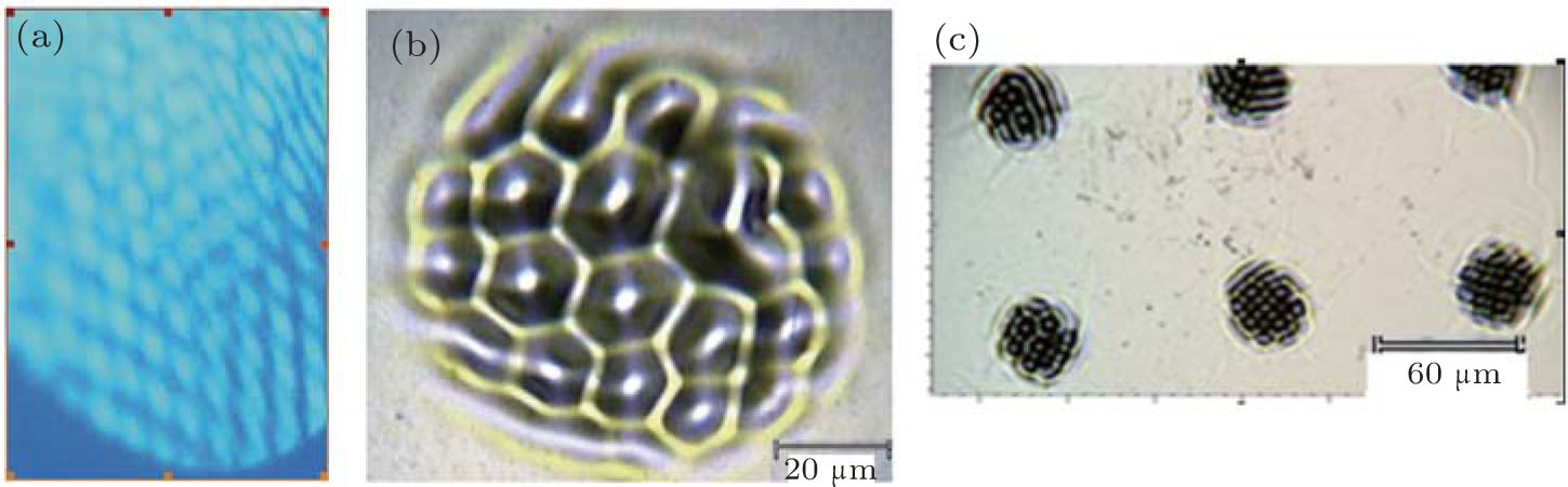
We fabricated a plasma cavity (diameter: 20 μ m∼ 60 μ m) array (interval: 100 μ m) with Si– Yb layers (Yb film of 15 nm) on silicon by depositing an SiO2 interlayer of 6 nm (to prevent the recombination of carriers at the Yb metal surface while maintaining strong cavity plasma fields in the silicon) as shown in Fig. 1(a). Room-temperature emission measurements were carried out on the plasma cavity array under a laser excitation source. Figures 1(b) and 1(c) show the bright visible light emissions from the structure under ns-pulsed Nd:YAG lasers at 532 nm and 1064 nm, respectively, which occurs in ball-shape light with plasmonic emission characteristics related to the distribution of plasma wave vector KF. The photonic energy in plasmonic emission has a wider range (white light), which is higher than the photonic energy in pumping at 1064 nm. The structure and composition of the Yb film are studied by TEM analysis in Fig. 2, which shows the bulge structure due to the mismatch between Si and Yb atoms in the Yb film surface. The inset in Fig. 2 shows the spectrum indicating the compositions Si and Yb in the film.
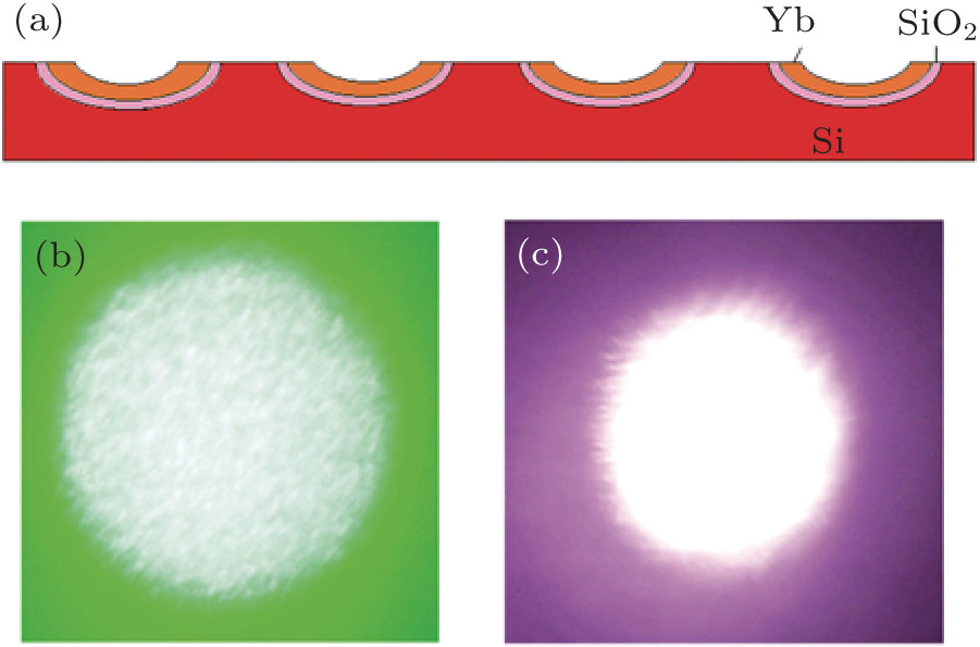 | Fig. 1. (a) Plasma cavity array with Si– Yb layers (Yb film of 15 nm) on silicon by depositing an SiO2 interlayer of 6 nm, (b) plasmonic emission in the cavity under ns-pulsed Nd:YAG laser at 532 nm, and (c) plasmonic emission in the cavity under ns-pulsed Nd:YAG laser at 1064 nm. |
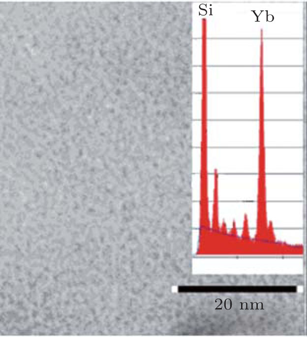 | Fig. 2. TEM image of the Yb film surface, with the inset showing the energy spectrum that indicates the compositions Si and Yb contained in the film. |
The plasma frequency (
It is interesting that in the Purcell cavity, there are several effects on the plasmonic emission: the first effect is the low-dimensional plasma effect which makes the band gap of plasmon narrower or disappear, which is the same as liquid metal which is easy to excite in the cavity; the second effect is to shorten the radiation lifetime for higher emission efficiency because of the resonance and coupling between plasmon and photon, meanwhile the relaxation time is lengthened in the plasma standing wave in the cavity.
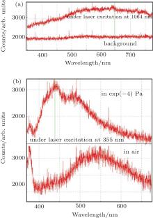
Figure 3(a) shows the plasmonic emission spectra under ns-pulsed Nd:YAG laser at 1064 nm in the Purcell cavity, in which a broad emission band occurs due to a broad distribution of electrons density in the plasma cavity. In the process, a persistent plasma plume is kept by controlling the intensity of the excitation laser, whose threshold is lower in plasmonic emission in the cavity.
 | Fig. 3. (a) Plasmonic emission spectra under ns-pulsed Nd:YAG laser at 1064 nm in the Purcell cavity, and (b) plasmonic emission spectra in air and in a vacuum under the excitation of the third harmonic of ns-pulsed Nd:YAG laser at 355 nm in the Purcell cavity. |
Figure 3(b) shows the plasmonic emission spectra under the excitation of the third harmonic of ns-pulsed Nd:YAG laser at 355 nm in the Purcell cavity, in which a broad hot luminescence band occurs in air because hot carrier emission competes with intraband relaxation, and in a vacuum, several characteristic peaks related to the intraband relaxation of Si– Yb structure appear in the plasma cavity. Here, the photoluminescence emission is enhanced because of the coupling with the plasmon. The plasmon frequency in the Purcell cavity could be described as[8, 13]

Here, the energy band gap disappears, which results in the fact that it is easy to excite by photons and hot carriers for emission.[13, 14]
As shown in Fig. 4, in the Purcell cavity the radiation lifetime is shortened to 100 ns in the transient time-response spectrum, which could be efficient for enhancing the emission. Generally speaking, the radiation lifetime is about 10 μ s in silicon with an indirect band gap.
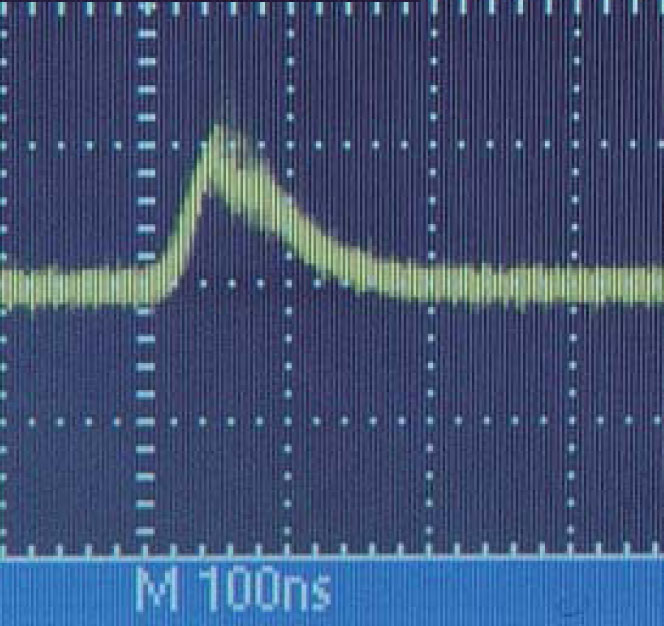 | Fig. 4. Transient time-response spectrum, showing that the radiation lifetime is shorted to 100 ns. |
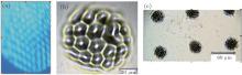
In the Purcell cavity, the plasma standing wave with some resonant modes is built by the interaction between plasmon and photon from the beam of the third harmonic of ns-pulsed Nd:YAG laser (355 nm) as shown in Fig. 5(a). Here, the period lattice structure image could be displayed by amplifying the Talbot reflection effect.[15, 16] This lattice structure of the plasma may be similar to the Wigner crystal structure.[17– 19] Figures 5(b) and 5(c) show the structures remaining in the cavity and in the cavity array after the interaction. The plasmonic energies Ep in quantized cavity modes could be given by

where Δ is the cavity scale, (p − eA) is the plasmonic momentum, and ε is the dielectric constant of the medium.[20]
 | Fig. 5. (a) Lattice structure image in the plasma standing wave displayed by amplifying the Talbot reflection effect, (b) and (c) the structures remaining in the cavity and in the cavity array after the interaction. |
In the Purcell cavity, the shorter radiation lifetime could be obtained in the plasma wave, which results in the enhancement of the plasmonic emission. Meanwhile, the relaxation time is lengthened, which could be observed in interference measurement between different pulses. Through increasing the number of laser pulses per second, the interferences of much more pulses with relaxation pulses could be built until the formation of finer lattice structures in the plasma standing wave in the cavity. It is very interesting that the diffraction pattern of the plasma lattice structure, induced by nanosecond pulses is observed in the Purcell cavity of silicon. Figure 6 shows the forming process of the diffraction pattern on the plasma lattice structure, induced by ns-pulsed laser at 1064 nm at different repetition rates of pulses, respectively at 1000, 2000, 3000, and 4000/s related to Figs. 6(a)– 6(d), in which the plasmonic emission occurs in the light center spot. It is discovered that the spatial frequency 1/d of the plasma period structure ranges from 1/100 nm to 1/20 μ m due to the quantized cavity modes in the plasma standing wave, induced by the laser pulses in the cavity, in which higher spatial frequency is obtained by increasing the pulses number per second, which could be explained by considering the plasma standing waves with higher order harmonic modes induced by multiple pulse interference due to photon delay in the cavity. It is useful to control the process of preparing the micro-nanostructures on silicon.
The process of inducing the plasma standing wave by laser pulses in the cavity could be described by the relation: L (interference length)/(Δ T) (interference time) = Σ (constant), in which the photons belong to the same quantum state when S (characteristic scale)/(Δ t) (interval time of pulses) is smaller than Σ , where the shorter interval time of pulses Δ t relates to the smaller characteristic scale S in the plasma cavity. The pulse interference in the same quantum state could induce a plasma standing wave with higher order harmonic modes to produce the finer lattice plasma structures with the higher spatial frequency in the cavity.
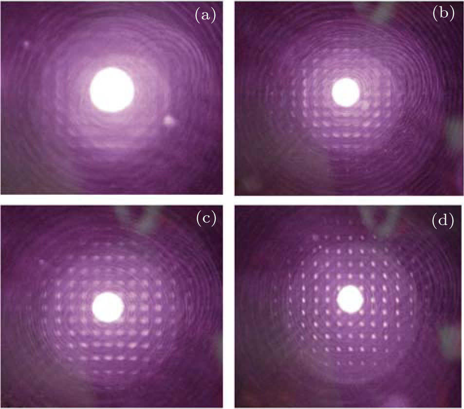 | Fig. 6. Diffraction patterns of the plasma lattice structures, induced by nanosecond laser pulses, at the repetition rates of (a) 1000/s, (b) 2000/s, (c) 3000/s or (d) 4000/s. |
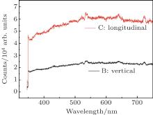
The measurements of polarization-dependent emission are carried for understanding the interplay between silicon photon and plasmon resonance in the Purcell cavity for efficient emission. The low-dimensional plasma wave in the Purcell cavity belongs to the longitudinal wave, [16] so it could be observed that the longitudinal polarized emission is stronger than the emission of vertical polarization because of resonant plasmons in the cavity as shown in Fig. 7. It is found that the switch of the plasmonic emission is built by changing the polarization between vertical and longitudinal directions. Here, it is demonstrated that the coupling of the longitudinal plasma wave enhances the longitudinally polarized emission.
 | Fig. 7. Longitudinally polarized and vertically polarization emission spectra in the plasmonic cavity under 20-ns pulsed laser at 532 nm. |
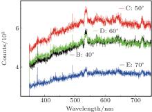
Figure 8 shows the plasmonic emission characteristics depending on angle direction in emission, in which the intensity of the plasmonic emission along the angle direction of about 50° with respect to the perpendicular direction is larger.
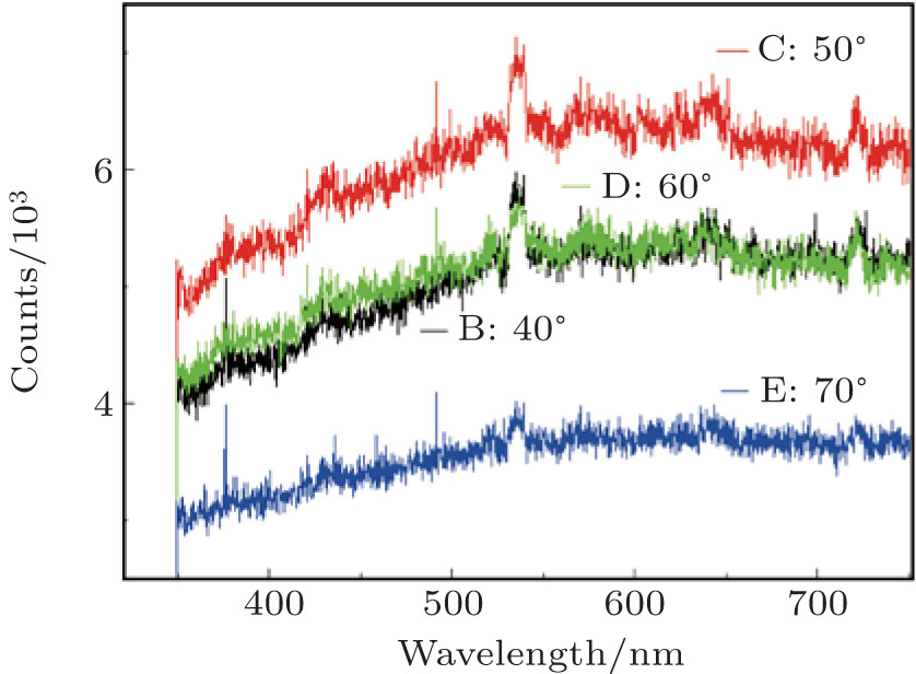 | Fig. 8. Plasmonic emission spectra with different angle directions under ns-pulsed laser at 532 nm. |
In this work, it is demonstrated that the low-dimensional plasma in the Purcell cavities array could have stronger visible light of plasmonic emission and enhance photoluminescence at room temperature from ‘ bulk-sized’ silicon, which provides an interesting test bed to study complex physical processes and could lead to new properties in engineered materials. The periodic diffraction patterns of the plasma lattice structures in the Purcell cavity are observed. The plasma standing wave in the cavity could be used to fabricate micro-nanostructures on silicon. The plasma lattice structures in the cavity may be similar to the Wigner crystal structure. The transient time-response spectrum shows the speeding of the radiation lifetime in the cavity. The lengthening of the relaxation time in the cavity is demonstrated by the interference between pulses in the standing wave of the cavity. The ability to obtain visible light emission from silicon devices, which are compatible to the length scales in current electronics, opens up a new way to integrate active silicon-based photonics with other conventional functionalities.
| 1 |
|
| 2 |
|
| 3 |
|
| 4 |
|
| 5 |
|
| 6 |
|
| 7 |
|
| 8 |
|
| 9 |
|
| 10 |
|
| 11 |
|
| 12 |
|
| 13 |
|
| 14 |
|
| 15 |
|
| 16 |
|
| 17 |
|
| 18 |
|
| 19 |
|
| 20 |
|