
Superscattering-enhanced narrow band forward scattering antenna
[Hu De-Jiaoa), b), c) , Zhang Zhi-Youa), b), c) , Du Jing-Lei†a), b), c)  ]
]
]
|
|


†Corresponding author. E-mail: dujl@scu.edu.cn
*Project supported by the National Natural Science Foundation of China (Grant No. 61377054), the Collaborative Innovation Foundation of Sichuan University, China (Grant No. XTCX 2013002), and the International Cooperation and Exchange of Science and Technology Project in Sichuan Province, China (Grant No. 2013HH0010).
We present a narrow band forward scattering optical antenna which is based on the excitation of distinctive whispering gallery modes (WGMs). The antenna is composed of three coaxial cylinder layers: a dielectric layer is sandwiched between a metallic core and cladding. Owing to the destructive interference between the scattering of the outer metallic cladding and the WGM in the backward direction, the power flow in the forward direction is increased. Simulation and analysis show that in proper geometry conditions, the cavity can be tuned into a superscattering state. At this state, both the zeroth and the first order of WGM are excited and contribute to the total scattering. It is shown that the power ratio (power towards backward divided by power towards forward) can be enhanced to about 27 times larger than that for a non-resonant position by the superscattering. Owing to the confinement of the cladding to WGMs, the wavelength range of effective forward scattering is considerably narrow (about 15 nm).
Directional scattering antenna with a narrow band is crucial for applications in nanophotonics, such as high sensitive optical switch and biosensor, narrow band nano-scale filter, etc. The directional scattering based on the interaction between electric and magnetic modes, which was firstly introduced by Kerker et al. in 1983, [1] is observed in core– shell nano-structures[2– 6] and dielectric nano-particles.[7– 9] It was also reported that the scattering direction of a single structure can be controlled by Fano resonance.[10, 11] In recent years, directional radiation of nano-scale optical antennas has attracted more and more attention and many excellent structures have been proposed. The directional radiation is mostly due to the interaction between two or more radiation modes, [12– 17] where the most famous example is the Yagi– Uda antenna.[15, 16, 18, 19] It was reported that the unidirectional side scattering of light can be realized via a single V-shaped nano-antenna, where two radiation dipoles on the antenna interact with each other, leading to suppressed and enhanced radiation towards two opposite directions.[16] However, the effective bandwidth of the directional scattering of these designed antennas has not yet been discussed. Generally speaking, the bandwidth can be considerably large in order to maintain the higher radiation efficiency. How to design the new narrow bandwidth directional antenna with both high radiation efficiency and high quality factor is a challenge.
In this paper, a directional scattering antenna is presented. We utilize the confinement of a metal cladding to the resonant field to reduce the radiation rate of each resonance mode, thus to reduce the bandwidth. On the other hand, the total scattering efficiency is preserved through the superscattering phenomenon. The antenna has the configuration of a nanowire coaxial cable, consisting of three concentric layers: a high permittivity dielectric ring layer sandwiched between a metallic core and cladding. According to its cylindrical cross section, “ coaxial cylinder antenna (CCA)” will be used to refer to the antenna hereafter. The CCA can support whispering gallery modes (WGMs) which are related to plasmonic waveguide modes in the dielectric layer.[20, 21] The interference between the scattering of the metallic cladding and the resonance scattering of WGMs results in quenched total backward scattering, as a consequence, the forward scattering is strengthened. The confinement of the cladding layer to WGMs weakens the radiation efficiency, thus increasing the quality factor and resulting in a narrow resonance bandwidth. The weakened radiation may lead to ineffective forward scattering. However, this inefficiency can be compensated through the superscattering phenomenon, where both the zeroth and the first order WGMs are excited at the same wavelength[22] and contribute to the forward scattering. We show that effective forward scattering can be maintained within a band width of about 15 nm.
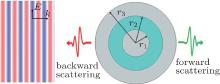
The cross section of the CCA is shown in Fig. 1 and is characterized by the geometrical parameters: r1, r2, and r3. This structure can support the surface plasmon waveguide mode in the dielectric layer.[20] The propagating surface plasmon waveguide mode in the dielectric ring forms WGMs. Under the illumination of a plane transverse magnetic (TM) wave in the leftward direction, the scattering amplitude of the CCA can be decomposed into two parts: the background scattering of the metallic cladding and the radiation of WGMs. The background acts as a super-radiant state which has a broad scattering peak while the WGM plays the role of a sub-radiant state. The phase of the WGM radiation changes rapidly near the resonance, which leads to constructive and destructive interference between the background and WGM radiation, resulting in the Fano-type scattering spectrum.[23– 25] If the resonant frequency of the super-radiant state is the same as that of the sub-radiant state, the Fano profile turns into a Lorentz profile with a scattering minimum (analogous to electromagnetically induced transparency, EIT).[26– 28] The destructive interference in the backward direction enhances the energy propagating towards the forward direction. This phenomenon is validated by full vector simulation. The simulation is conducted by using the COMSOL software in a two-dimensional (2D) simulation case on the assumption that the normal dimension is uniform (i.e., nanowire). The forward (backward) scattering cross section is calculated by integrating the energy flow over the right (left) half-circle, and the result is divided by the incident light intensity [Fig. 1], and is denoted as σ f (σ b). Thus the total scattering cross section which is related to the total power flowing through the boundary of CCA, is the sum of σ f and σ b. In the calculations, the metal layer is set as silver with a permeability of 1, and the complex permittivity comes from Ref. [29]. The permittivity of the dielectric layer is 12.96. These geometric parameters are r1 = 70 nm, r2 = 140 nm, and r3 = 190 nm respectively, making the thickness of the cladding t = 50 nm.
 | Fig. 1. Schematic diagram of the cylinder scatter composed of a dielectric layer sandwiched between the metallic core and cladding. |
The spectra of σ f and σ b are calculated and shown in Fig. 2(a) as black and red dash– dotted curves (normalized by 2λ /π ). Meanwhile, the integral of the square of the modulus of the electric field over the dielectric layer is calculated by using ∫ | E| 2dS, which is proportional to the total stored energy. The results are shown in Fig. 2(a) as a blue dotted curve. It is revealed that the stored energy reaches the maxima at λ = 749.9 nm and 757.4 nm respectively. The corresponding electric field distributions are shown as insets in Fig. 2(a), which indicate that these two peaks are related to the first order (left) and zeroth order (right) WGMs respectively.[20] The peaks related to these two modes in the forward scattering spectra overlap each other and are difficult to identify. However, two dips emerge in the backward spectrum at 749.9 nm and 757.7 nm, implying that the backward scattering is suppressed and these WGMs are responsible for the suppression. The ratio between the forward and the backward scattering cross section (σ f/σ b) as a function of wavelength is shown as a solid blue dash– dotted curve in Fig. 2(b), where these two peaks sit at 750.2 nm and 757.4 nm, corresponding to these dip positions in the backward spectrum. The radiation patterns related to these peaks are shown in Fig. 2(c) as solid blue solid and red dashed curves. In addition, the pattern for an off-resonance wavelength of 761.4 nm is also shown in the same figure with a green dotted curve (σ f/σ b = 1.5). It can be observed that the forward scatterings for λ = 750.2 and 757.4 nm are enhanced compared with that at the off-resonant position (761.4 nm). The enhancement manifests as larger forward far-field power flow and less backward side lobes in consequence of the suppression of the backward scattering [Fig. 2(c)].
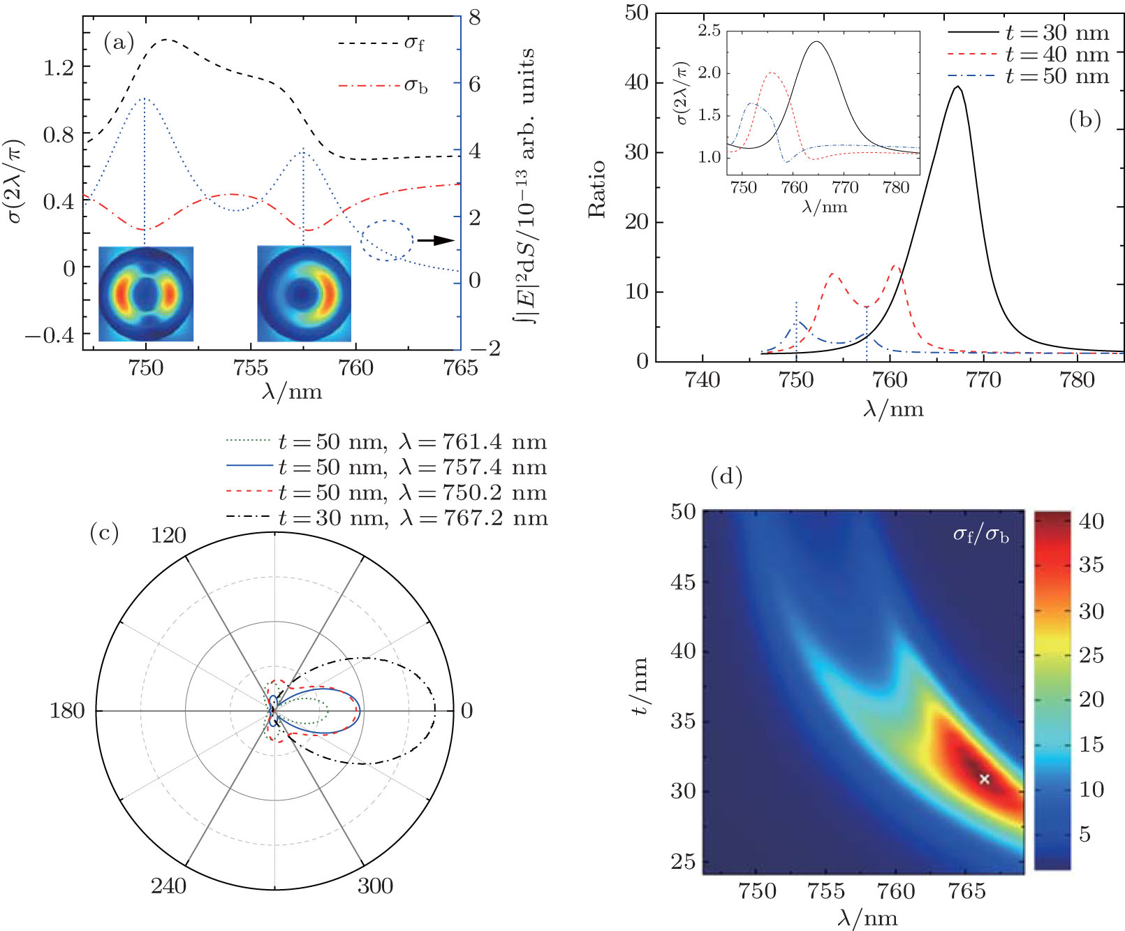 | Fig. 2. (a) Forward (σ f, black dashed) and backward (σ b, red dash dotted) scattering cross section of the CAA with r1 = 70 nm, r2 = 140 nm, and r3 = 190 nm (t = 50 nm). The blue dotted line represents the integral of the square of the modulus of the electric field over the dielectric layer, which is proportional to the stored energy. The electric field distributions within the CCA are displayed under their corresponding peaks as insets. (b) The variations of ratio between forward and backward scattering cross section (σ f/σ b) with wavelength for t = 30 nm, 40 nm, and 50 nm respectively. (c) Radiation patterns (power to the far field) for off-resonance position (green dotted line) at t = 50 nm and ratio (σ f/σ b) peak positions (blue solid and red dashed for t = 50 nm, black dash– dotted for t = 30 nm). (d) The map of the ratio between forward scattering and back scattering against the thickness of the cladding and wavelength. |
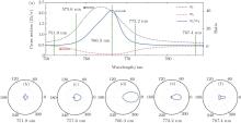
By keeping r1 and r2 fixed and varying r3, the ratio spectra for cladding thickness values of 30 nm and 40 nm are calculated and plotted in Fig. 2(b) as well. From the figure, it is shown that these two peaks become closer and higher as t changes from 50 nm to 40 nm, and further become a totally overlapped peak at 767.2 nm when t = 30 nm. The maximum value of the ratio changes from 5.6 to 14 and further reaches 40 when t varies from 50 nm to 30 nm. The above facts manifest that by modifying the cladding thickness, the CCA can be tuned into the superscattering state, at which both the zeroth and the first order WGMs are excited at the same wavelength. At that wavelength, the energy is scattered through multiple resonance channels (two channels here), which leads to a scattering cross section larger than 2λ /π .[22] As shown in the inset of Fig. 2(b), the maximum of the total scattering cross section grows from 1.6 × (2λ /π ) to 2.4 × (2λ /π ) with t changes from 50 nm to 30 nm, which is evidence of the superscattering. The radiation pattern of the CCA at a t of 30 nm and a wavelength of 767.2 nm is shown as a black dash– dotted curve in Fig. 2(c). The pattern shows a much better forward scattering property (almost no visible side lobes) than the blue solid and red dashed ones which correspond to these peak positions at t = 50 nm. Figure 2(d) shows the map of the cross section ratio as a function of the thickness of the cladding and wavelength. The variation of the ratio peak along with the thickness is clearly seen, where the decreasing of thickness leads to red shifts and increases of these peaks. The largest ratio (41) is found at t = 31 nm, which is about 27 times larger than that for the non-resonant position mentioned above. The corresponding spectra are shown in Fig. 3(a), showing that the forward (backward) scattering cross section has only one peak (dip) larger than 2 × (2λ /π ), proving the emergence of superscattering. The ratio reaches its maximum at a wavelength of 766.3 nm. Radiation patterns corresponding to the peak and some other positions marked with green vertical dashed lines in Fig. 3(a) are shown in Figs. 3(b)– 3(f). The CCA at 766.3 nm exhibits the best forward scattering property. When the wavelength shifts away from the peak to 757.6 nm and 772.2 nm, where the ratios are both 1/8 of the maximum value, the power flow towards forward decreases to about half the maximum (Figs. 3(c) and 3(e)). The relevant band width is as narrow as about 15 nm. The forward scattering becomes less effective at wavelengths of 751.9 nm and 787.4 nm, where more energy is scattered through these side lobes in the backward direction (Figs. 3(b) and 3(f)). These results manifest that the effective forward scattering band width is considerably narrow due to the cladding confinement. Meanwhile, the forward scattering efficiency can be guaranteed through the superscattering phenomenon.
 | Fig. 3. (a) Forward (σ f, black dashed) and backward (σ b, red dash– dotted) scattering cross section of the CAA with r1 = 70 nm, r2 = 140 nm, and r3 = 171 nm (t = 31 nm). Blue solid curve shows the spectrum of the corresponding cross section ratio. (b)– (f) Radiation patterns (to the far field) corresponding to these positions marked with green vertical dashed lines in panel (a). All curves are plotted with the same axis scale. |
In this work, we demonstrate a narrow band forward scattering antenna. The narrow band stems from the confinement of the metal cladding to the WGM, and the forward scattering is due to the destructive interference between the background scattering and the scattering of the WGM. The forward scattering efficiency is further enhanced by the superscattering phenomenon. The superscattering of a CCA compensates the loss in efficiency brought in by the cladding, which provides a way to solve the contradiction between the radiation efficiency and the quality factor of a single resonance mode. In our work, we find an alternative method to realize narrow band directional scattering antenna and guarantee the scattering efficiency at the same time. It has the potential to open up new design capabilities and can be applied to sensitive optical switches, narrow band optical filters, and wave guiding devices.
| 1 |
|
| 2 |
|
| 3 |
|
| 4 |
|
| 5 |
|
| 6 |
|
| 7 |
|
| 8 |
|
| 9 |
|
| 10 |
|
| 11 |
|
| 12 |
|
| 13 |
|
| 14 |
|
| 15 |
|
| 16 |
|
| 17 |
|
| 18 |
|
| 19 |
|
| 20 |
|
| 21 |
|
| 22 |
|
| 23 |
|
| 24 |
|
| 25 |
|
| 26 |
|
| 27 |
|
| 28 |
|
| 29 |
|