

Absorption enhancement in thin film a-Si solar cells with double-sided SiO2 particle layers
[Chen Lea), b) , Wang Qing-Kang†a)  , Shen Xiang-Qian
a) , Chen Wenb) , Huang Kuna) , Liu Dai-Minga) ]
, Shen Xiang-Qian|
|


†Corresponding author. E-mail: wangqingkang@sjtu.edu.cn
*Project supported by the National High-Tech Research and Development Program of China (Grant No. 2011AA050518), the University Research Program of Guangxi Education Department, China (Grant No. LX2014288), and the Natural Science Foundation of Guangxi Zhuang Autonomous Region, China (Grant No. 2013GXNSBA019014).
Light absorption enhancement is very important for improving the power conversion efficiency of a thin film a-Si solar cell. In this paper, a thin-film a-Si solar cell model with double-sided SiO2 particle layers is designed, and then the underlying mechanism of absorption enhancement is investigated by finite difference time domain (FDTD) simulation; finally the feasible experimental scheme for preparing the SiO2 particle layer is discussed. It is found that the top and bottom SiO2 particle layers play an important role in anti-reflection and light trapping, respectively. The light absorption of the cell with double-sided SiO2 layers greatly increases in a wavelength range of 300 nm–800 nm, and the ultimate efficiency increases more than 22% compared with that of the flat device. The cell model with double-sided SiO2 particle layers reported here can be used in varieties of thin film solar cells to further improve their performances.
With the rapid development of the photovoltaic industry, thin film amorphous silicon (a-Si) solar cells have attracted much attention due to the advantages of saving materials and reducing costs.[1– 3] Unfortunately, the power conversion efficiency (PCE) of thin film a-Si solar cells is limited because of their thin absorption layers.[4] Increasing the thickness of the light absorption layer can effectively enhance the power conversion efficiency, but leads to high manufacturing costs. Besides, a thicker absorption layer also results in enhancement of the cell series resistor, which ultimately reduces the fill factor and the short current density.[5] So far, a potential way to solve these problems is to trap the incident light within the absorption layer with some random or periodic texture structures, such as plasma grating, [6] photonic crystal, [7] nanowire, [8] nanohole, [9] nanodome, [10] and nanocone.[11] Another feasible approach is to add an external optical element which can reduce the surface reflectivity and make more escaped light return to the absorption layer.[4] However, such light trapping methods still have some problems. For instance, the random or periodic texture structures can easily result in irreparable defects or damages, which will restrict the light absorption and affect the performance of the solar cell. Moreover, the fabrication of such structures always needs expensive equipment and complex technology such as lithography, sputtering, and etching, which will directly increase the cost of the products. So it is necessary to develop non-destructive and low-cost anti-reflection (AR) and light trapping structures for enhancing the light absorption and the PCE of solar cell.
The SiO2 particle has unique photonic properties and is widely used in many photovoltaic devices. It can effectively increase the PCE of a solar cell through a suitable combination process.[12– 16] For example, Jonathan Grandidier et al.[15] have experimentally and theoretically demonstrated that the PCE of a-silicon solar cell with a top SiO2 layer was significantly higher than that of a flat device, and the Cui Yi research group has also shown that a thin film a-silicon solar cell with a bottom SiO2 layer exhibited 42% higher absorption than the corresponding flat cell. Until now, however, there have been few reports about the thin film a-Si solar cell with both top and bottom monolayer SiO2 particles. In this paper, the absorption performance and the ultimate efficiency of a thin film a-Si solar cell with double-sided (top and bottom) SiO2 particle layers are investigated by Finite Difference Time Domain (FDTD) numerical simulation.
In our approach, the core algorithm of the calculation is based on the FDTD simulation, which is a state-of-the-art method for solving Maxwell’ s equations in complex geometries. Four kinds of thin film a-Si solar cell models are designed to figure out the light absorption enhancement performance of the cells with “ top and bottom” SiO2 layer, as shown in Fig. 1.
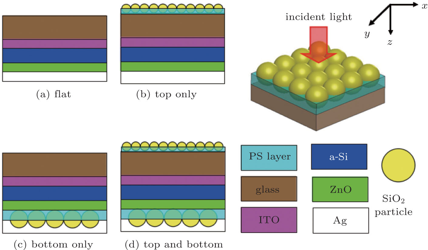 | Fig. 1. 2D models of the thin film a-Si solar cell: (a) without SiO2 layer, (b) with top SiO2 layer, (c) with bottom SiO2 layer, and (d) with both top and bottom SiO2 layers. |
Figure 1(a) depicts the two-dimensional (2D) model of a typical single-junction flat thin film a-Si solar cell device.[17] The silver (Ag) serves as a back contact electrode, and a zinc oxide (ZnO) layer with a thickness of 40 nm is sandwiched between the Ag layer and the a-Si layer in order to avoid diffusion between them and enhance the back reflection. An indium tin oxide (ITO) layer with a thickness of 70 nm is used as a transparent conducting front contact and also acts as an AR coating layer. The a-Si layer is about 235-nm thick as the absorption layer, including p-a-Si (15-nm thick), i-a-Si (200-nm thick), and n-a-Si (20-nm thick). As shown in Figs. 1(b)– 1(d), SiO2 particles are placed on the top or at the bottom of the cell and fixed by a polystyrene (PS) layer. In order to study the response mechanism of these cells with the SiO2 layer, we perform the three-dimensional (3D) electromagnetic simulations and compare the results with those of the flat device. A broadband pulse plane wave with the electric field polarized along the x axis is projected with normal incidence on the cells, and the fields are monitored in a wavelength range of 300 nm– 800 nm. This range corresponds to the energy spectrum of the sun, which is always considered for the material of a-Si.
The values of the extinction coefficient and the refraction index of the materials in the solar cell model, including a-Si, SiO2, ITO, ZnO, and Ag are obtained from the refractive index database.[18] For convenience, nglass = 1.5 and nPS = 1.6 are selected as the refractive indices of glass and PS layer, respectively. Their extinction coefficients are neglected here, because they are equal to zero. The diameter of the bottom SiO2 particle is twice that of the top one.
To quantitatively estimate the AR and light trapping capability of the proposed SiO2 layer, the ultimate efficiency (η ) is calculated by the following equation:[19]
where λ g = 730 nm is the band gap of a-Si (Eg = 1.7 eV), λ is the wavelength of incident light, I(λ ) is the solar energy density spectrum of American Society of Testing Materials (ASTM) (air mass 1.5, direct normally incident and circumsolar spectrum), [20] and A(λ ) is the absorption spectrum of the solar cell, which is given as follows:[21]

where R(λ ) is the reflection spectrum, which can be easily obtained by the FDTD simulation. The T(λ ) can be ignored when the back reflective layer Ag is thick enough (more than 100 nm). Here, we just focus on the solar spectrum (300 nm– 4000 nm) mainly because the solar irradiance could be neglected when the solar spectrum is smaller than 300 nm or larger than 4000 nm.
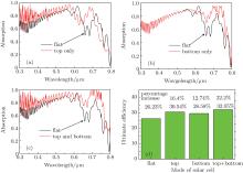
The performances of these three solar cells with different SiO2 layers are shown in Fig. 2, comparing with that of the flat model under the condition of normal incidence by TM plane wave. The two curves represent the absorption spectra for the flat model and the corresponding SiO2 layer models respectively as shown in Fig. 1. In these models, 300 nm and 600 nm are selected as the diameters of top and bottom SiO2 particles, respectively. It is a good choice which will be proved later. Finally, the ultimate efficiency of each model is calculated by Eq. (1).
 | Fig. 2. (a)– (c) Comparison of absorption spectrum between the models with SiO2 layer and the flat model. (d) Comparison of ultimate efficiency between these models and the flat model, showing that compared with the flat model, the “ top only” , the “ bottom only” , and the “ top and bottom” models increase the ultimate efficiencies by 16.4%, 12.7%, and 22.2%, respectively. |
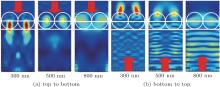
The absorption spectrum of the cell model with a “ top only” SiO2 layer is shown in Fig. 2(a). Compared with the absorption spectrum of the cell of the flat model in Fig. 1(a), one can observe substantial absorption enhancement in short wave (300 nm– 600 nm). The ultimate efficiency is 30.54% for the “ top-only” model, which is 16.4% higher than that of the flat model. The contribution to light absorption enhancement originates mainly from the AR effect of the top SiO2 layer. The top SiO2 layer can suppress the front surface optical reflection, as the surface geometry of the SiO2 particle provides an averaged graded index from air to the glass surface. The cross section radius of the SiO2 particle increases from zero to its maximum at the planar film surface. Moreover, a high aspect ratio array is preferred to provide a smooth index transition.[22] However, the absorption enhancement is not obvious in a long wavelength range of 600 nm– 800 nm, which is because the period of the top SiO2 particle is much smaller than the wavelength. In this case, the long wavelength light will mainly produce specula reflection, so the reflection effect will be dominant and the influence of the top SiO2 layer can be neglected. Therefore, the structural feature of the top SiO2 particle is optimal for anti-reflection and sub-optimal for light trapping. Figure 3(a) shows the power field distributions. When the light beams come from air to glass (from top to bottom, as indicated by red arrows) with the wavelengths of 300 nm, 500 nm, and 800 nm, they will be scattered on the surfaces of the SiO2 particle, and the radii of their cross sections increase from zero at air to maximum at the PS layer surface. So the SiO2 particle can suppress the reflection of light and the transmittance of the incident light will increase. Conversely, when the light beams coming from the bottom glass tend to enter into top air, a part of the light beams will be reflected back to the glass again. The reflected light beams will be absorbed by the solar cell again. The power field distributions are shown in Fig. 3(b) when the light beams come from glass to air (from bottom to top). Hence the light trying to escape from the SiO2 surface will be restricted. In Figs. 3(a) and 3(b), we can find that the wavelengths of incident light are closer to the diameters of the SiO2 particle, and the light is more sensitive. So the AR effect in the short wavelength range is obviously more effective than in a long wavelength.
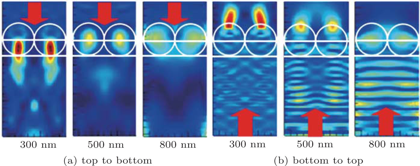 | Fig. 3. Cross-sectional power field intensity distributions of the “ top only” SiO2 layer at different incident light wavelengths, showing the light beams coming from air to glass (from top to bottom) (a), and from glass to air (from bottom to top) (b). |
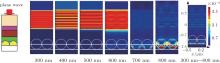
The absorption spectrum of the cell model with a “ bottom only” SiO2 layer is shown in Fig. 2(b). In this model, the period of the bottom SiO2 grating is 600 nm. One can find that the ultimate efficiency is up to 29.58%, and the percentage enhancement is 12.7%. When the wavelength is less than 600 nm, the absorption spectrum curve almost coincides with that of the flat model, but when the wavelength is greater than 600 nm, we observe significant absorption enhancement. This proves that the bottom SiO2 particle layer does not contribute to AR, but it is an optimal strategy for light trapping, especially in the long wavelength range. Compared with the absorption spectrum of the top SiO2 layer for AR, the absorption spectrum in Fig. 2(b) shows that the absorption enhancement by light trapping is primarily in the long wavelength range in which the silicon absorption is weak. Light trapping relies on the excitation of guided resonances and therefore a careful choice of the texture periodicity is important. The requirement of periodicity depends on two considerations. One is that more guided resonances lead to higher absorption, for which a larger period is preferred. The other is that each of the guided resonances cannot couple and leak to many external channels, for which a smaller period is preferred. Considering the tradeoff between the above two requirement considerations, the optimal periodicity for light trapping should be close to the targeted wavelength.[23] For a-Si material, light trapping is important for the wavelength range of 600 nm– 800 nm. Therefore, we expect that the optimal periodicity is 600 nm– 800 nm, and the wavelength in the normally incident plane wave is efficiently coupled to guided resonances, as shown in Fig. 4. The power field distributions of the plane wave in the bottom SiO2 particle are different in different wavelength ranges. It means that the light trapping is primarily in a long wavelength range of 600 nm– 800 nm. Light trapping relies on the excitation of guided resonances, and therefore the bottom SiO2 layer is a good choice for enhancing the light absorption.
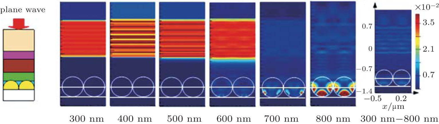 | Fig. 4. Cross-sectional power field intensity distributions of the “ bottom only” SiO2 layer at different incident light wavelengths. |
According to the above analyses, one can see that the top and the bottom SiO2 layers obviously enhance the absorptions of short wavelength and long wavelength, respectively. We need to enhance the absorption in the entire usable solar spectrum to obtain effective absorption enhancement. So we design the cell model with the “ top and bottom” SiO2 layers as shown in Fig. 1. The absorption spectrum of the “ top and bottom” model is shown in Fig. 2(c). Compared with the flat model, the “ top and bottom” model achieves a substantial absorption enhancement over the entire incident wavelength range (300 nm– 800 nm), the ultimate efficiency reaches up to 32.05%, and the percentage enhancement is 22.2%.
To further investigate the influence of the diameter of the SiO2 particle on the performance of the solar cell with “ top and bottom” SiO2 layers, the ultimate efficiencies with different diameters of top and bottom SiO2 particles are shown in Fig. 5. We can find that the ultimate efficiency gradually increases with the diameters of top and bottom SiO2 particles increasing, and becomes balanced finally. When dSiO2− top ≥ 300 nm and dSiO2− bottom ≥ 600 nm, the ultimate efficiency becomes a stable value. This result shows that our choices of parameters in the “ top and bottom” solar cell model are reasonable. The ultimate efficiency of our cell is not strongly dependent on the size of SiO2 particle when the diameters of top and bottom SiO2 particles are greater than 300 nm and 600 nm, respectively.
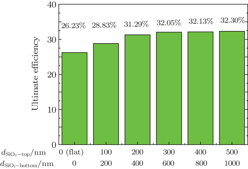 | Fig. 5. Ultimate efficiencies of the “ top and bottom” solar cells with the different diameters of top and bottom SiO2 particles. The 0-nm sample also represents the flat model. |
As a final remark, the SiO2 particle can be easily obtained by the hybrid reaction of ethanol, ethylsilicate (TEOS), and ammonia. The TEOS and ammonia are used as silicon source and catalyst, respectively. Generally, there are two common methods to fabricate the monolayer close-packed SiO2 particles on the surface of glass substrate. One is the Langmuir– Blodgett (LB) method which has been proved to be one of the most effective ways of assembling monolayer SiO2 particles.[23] The other is the wire-wound rod coating method, which is a simple coating method for assembling SiO2 particles on a flexible or inflexible substrate.[24] Polystyrene (PS) is a synthetic aromatic thermoplastic polymer which is widely used in solar areas. It can be easily melted into liquid by heating to 120 ° C. So there are two feasible schemes of experiment to prepare the SiO2 particles for nesting into the PS layer experimentally. One is that the close-packed SiO2 particle monolayers are assembled on the surface of the glass substrate at first, and then a PS layer is coated onto the glass wafer by a spin or spray method. This method is proved to be feasible by Chen et al.[25] The other is that the close-packed PS particle monolayer is first assembled on the surface of the glass substrate via rapid convection deposition, then the close-packed SiO2 particle monolayer is deposited on the top of PS particles, and finally the PS particles are melted into a planar layer via the heat treatment method. This method is also proved to be feasible by Yik– Khoon et al.[26]
In this paper, we design a thin film a-Si solar cell model with a “ top and bottom” SiO2 particle layer, and the absorption spectra and ultimate efficiencies are calculated by the FDTD numerical simulation. The results show that the top SiO2 particle layer can obviously enhance the absorption for a short wavelength, while the bottom SiO2 particle layer can obviously enhance the absorption for a long wavelength. Both the top and bottom SiO2 particles can obviously enhance the absorption for the short and long wavelength range (300 nm– 800 nm). Compared with the flat device, the “ top only” , “ bottom only” , and “ top and bottom” models can increase ultimate efficiencies up to 16.4%, 12.7%, and 22.2%, respectively. The light propagation shows that the top and bottom SiO2 layers of the cell separately play an important role in AR for short wavelength and light trapping for long wavelength. The ultimate efficiency of the “ top and bottom” SiO2 particle model cell is not strongly dependent on the size of SiO2 particle when the diameters of top SiO2 particles and the bottom SiO2 particles are greater than 300 nm and 600 nm, respectively.
| 1 |
|
| 2 |
|
| 3 |
|
| 4 |
|
| 5 |
|
| 6 |
|
| 7 |
|
| 8 |
|
| 9 |
|
| 10 |
|
| 11 |
|
| 12 |
|
| 13 |
|
| 14 |
|
| 15 |
|
| 16 |
|
| 17 |
|
| 18 |
|
| 19 |
|
| 20 |
|
| 21 |
|
| 22 |
|
| 23 |
|
| 24 |
|
| 25 |
|
| 26 |
|