


Tunable wideband absorber based on resistively loaded lossy high-impedance surface
[Dang Ke-Zheng, Shi Jia-Ming† , Wang Jia-Chun, Lin Zhi-Dan, Wang Qi-Chao]
, Wang Jia-Chun, Lin Zhi-Dan, Wang Qi-Chao]
|
|


†Corresponding author. E-mail: shijmeei@yahoo.com
A lossy high-impedance surface comprised of two layers of resistive frequency selective surfaces is employed to design a tunable electromagnetic absorber. The tunability is realized through changing the composite unit cell by moving the top layer mechanically. To explain the absorbing mechanism, an equivalent circuit model with an interacting coefficient is proposed. Then, simulations and measurements are carried out and agree well with each other. Results show that the complex structure with a thickness less than λ0/4 is able to achieve a wideband absorption in a frequency range from 5.90 GHz to 19.73 GHz. Moreover, it is tunable in the operation frequency band.
As is well known, the microwave absorber is very useful in a number of areas; for instance absorbers can be covered or coated on a conducting object to reduce the radar cross-section (RCS).[1] By now different kinds of microwave absorbing materials have been designed and applied, such as the famous Salisbury screen, [2] the circuit analog absorber, [3] etc. However, efforts to explore new methods of designing the absorbers have never been reduced. Since the perfect absorber was discovered in Ref. [4], developments in metamaterials have aroused much interest in designing various absorbers.[5– 9] As a typical kind of metamaterial, a high-impedance surface (HIS)[10] has an interesting in-phase reflection characteristic, which has been widely applied to the constructions of optical Fabry– Pé rot cavity, [11] microwave antennas, [12] etc. Recent years, several effective attempts have been made to increase the absorbing capability of electromagnetic absorbers based on HIS with ultrathin thickness less than λ /8, in which either lumped resistors between adjacent metallic patterns, [13] or a resistive frequency selective surface (FSS) composed of periodic resistive patterns are used.[14] Absorption bands of all the absorbers mentioned above are either narrow or wide, depending on their configurations, but not so flexible as the complex structures, once they have been manufactured. Tunable absorbers have been presented in Refs. [15] and [16], but exhibit narrow- band response (no more than 2 GHz).
In this paper we propose a wideband and thin absorbing structure based on lossy HIS loading resistive FSSs; moreover, the absorber is also tunable over the operation frequency range, which is realized by changing the composite unit cell through a combination between two overlapping layers of resistive frequency selective surfaces. To demonstrate the physical mechanism of the tunable absorption, an equivalent circuit model of the absorber is presented. Then simulations and experiments are carried out to verify the validity of the tunable wideband absorber.
For a HIS absorber, as analyzed in Ref. [17], the frequency and bandwidth of the resonant absorption greatly depend on the unit cell shape and the surface resistance of the patterns in the FSS. So, theoretically the absorber can be designed to be tunable by changing the pattern’ s shape or square resistance. However, the dimensions and the resistance values are settled once a layer of FSS has been fabricated. So we utilize two overlapped FSS layers to realize the change of the pattern’ s shape. As shown in Fig. 1, the absorbing slab is designed consisting of four layers. Three of them make up a conventional lossy HIS comprised of a resistive FSS (referred to as the second FSS) over a thin grounded dielectric panel. Meanwhile, at the top of the whole structure, the fourth one is still a layer of resistive FSS (referred as the top FSS). The top and second FSSs are both structured by periodically arranged resistive square rings with the same physical parameters. The rings are made of patterned resistive film with a proper surface resistance.
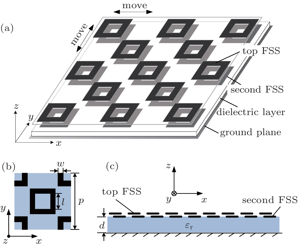 | Fig. 1. Three-dimensional sketch of the absorber, showing (a) oblique view, (b) top view of the unit cell, and (c) side view. Detailed dimensions: p = 22 mm, w = 2 mm, l = 6 mm, and d = 5 mm. |
Covering on the conventional lossy HIS, the top FSS contacts the second one, but is movable along the x and y directions separately or simultaneously. To move the top layer exactly, a mechanical device can be employed. As a result of the movements, the top FSS overlaps the second FSS in the HIS to a different extent. Take the two connecting FSSs as a whole, which means that the composite pattern is changeable though its two constituent elements are invariable. To show this point, in Fig. 2, assuming the two FSSs coincide originally we make the top resistive FSS have an increasing x-directional shift from 0 to 8 mm in steps of 2 mm corresponding to Figs. 2(a)– 2(e) respectively. Meanwhile, the second FSS keeps stationary below. The other situations when the top FSS moves along different directions and different distances are quite similar, so they will not be discussed here for concision. It is apparent that the composite pattern varies with the relative displacement between the two FSS layers, although each single FSS remains unchanged.
 | Fig. 2. Composite patterns with different displacements between the two FSS layers from 0 to 8 mm with a 2-mm step in x direction, corresponding to panel (a) to panel (e) respectively. |
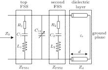
To get a better understanding of physical mechanism of the tunable absorption, an equivalent circuit model of the absorber is shown in Fig. 3. The circuit mainly consists of four parallel parts presenting four layers of the complicated structure and an interacting coefficient C12 between two FSS layers.
 | Fig. 3. Equivalent circuit model of the complicated structure. |
In this circuit model, the ground plane is presented as a short circuit in the rightmost parallel connection. Based on this approximation, the surface impedance Zd of the grounded dielectric layer has been calculated in Ref. [18], which is closely related to the layer’ s dielectric constant ɛ r and its thickness d.
The top and second resistive FSSs as shown in Fig. 3 are both presented by a series of RLC parameters as demonstrated in Ref. [14]. The surface impedance of FSS can be computed analytically as follows:

where n = 1, 2 correspond to the two FSSs respectively and ω is the angular frequency of the incident wave. Considering the fact that the top FSS has the same physical parameters as the second one as mentioned in the design, there actually are R1 = R2, L1 = L2, C1 = C2. But it should be pointed out that the parameters of these two FSSs could have different values resulting from quite different pattern shapes, different square resistances, etc. to make the design more flexible. Here, in this work, the sameness is just to simplify the design.
For an ideal composite unit cell, its constituents closely join together. In other words, the distance between the two FSSs should be zero. As the FSS could not exist in the case without any substrate, actually there is another dielectric layer between the two FSSs. In our design, its thickness is assumed to be so ultrathin that its impedance is negligible and not introduced into the circuit model. Nevertheless, the interaction between the two FSSs becomes non-negligible because of the ultra-close distance. To demonstrate this, we suppose that the coordinate is defined as Fig. 1(b), and make the top FSS move along the x-direction. As a result, the coupling area between adjacent edges of square rings separately on the top and second FSS increases with the movement as marked in Fig. 2. When the electric field of the incident microwave is parallel to the y-axis, the coupling area’ s increase will just lead to an increasing coupling capacitance between the top and second FSS layers. A similar situation happens when the top FSS has a y-directional displacement. As the equivalent inductance in HIS is not so affected by the variation of the composite pattern as the capacitance, [19, 20] here the coupling inductance is not taken into account. Consequently, the interacting coefficient C12 in the equivalent circuit model could be defined as the intercoupling capacitance between the top and second FSS unit cells.
Then, the impedance of the two FSSs as a whole can be represented as follows:

From the view of the coupling capacitance, the longer the distance between the two FSS layers, the smaller the value of the coefficient C12 is. That means the role of the C12 in formula (2) is less important and the influence of the coupling capacitance on the impedance ZFSS will be less. Besides, a long distance will not make the impedance of the spacer between the two FSSs neglected. The impedance of the spacer will also weaken the influence of coefficient C12. The circuit model should be modified by adding another piece of equivalent transmission line between the two parallel RLC circuits. As this paper focuses on the tunability of the absorber, the distance should be as short as possible. The situations of long distance between the two FSSs will not be discussed particularly.
For the absorber, the total surface impedance Zin equals the resulting impedance of the parallel connection of the composite FSS and the grounded dielectric slab, i.e.,

Then the reflection coefficient of the HIS absorber is obtained as

where Z0 is the impedance of the free space.
From the analysis above, the impedances ZFFS1, ZFFS2, and Zd are separately fixed once the absorber has been prepared, which apparently cannot result in any changeability in the absorbing performance. The only variable parameter is the interacting coefficient introduced by two overlapping layers of FSSs. Typically, it is the coupling capacitance C12 between the top and second FSSs, which leads to the tunability of the absorber, when there are a variety of relative displacements between these two FSS layers.
Computer simulation of this novel absorber is performed by employing commercial software, the CST Microwave Studio, with a finite difference time domain solver under a unit cell boundary condition. The absorber has the same size and material properties as stated above, but the material type of lossy FSS is set to be an ohmic sheet with a resistance of 70 Ω /sq. We obtain the simulation results as shown in Fig. 4, which gives the reflection loss over the frequency range from 4 GHz to 20 GHz corresponding to each composite pattern in Fig. 2. Here we assume that the incident electric field vector is perpendicular to the motion direction of the top FSS.
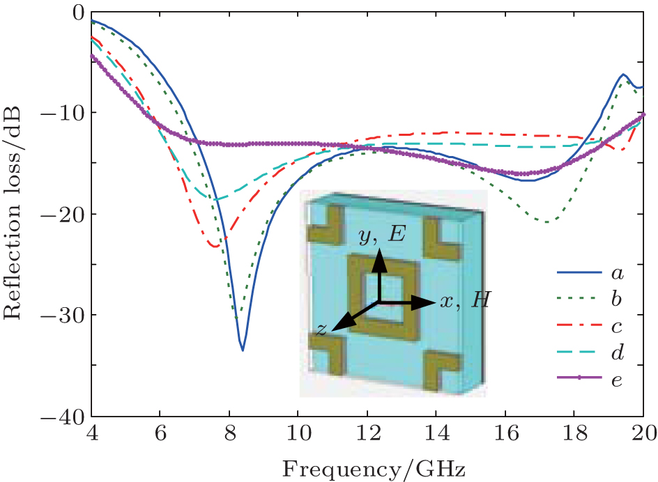 | Fig. 4. Simulated reflection losses of structure with different unit cells. |
From the simulation results, it is evident that the absorber proposed in this paper gives a tunable and wideband microwave absorbing performance. Each line in Fig. 4 almost has two absorption peaks, which are apparent or not, owing to two resonances within the operating frequency band. As a result, the absorber always has a wide absorbing band no matter how the composite unit pattern changes. Moreover, for different lines, the change in the absorbing performance of the absorber gradually happens along with the movement of the top FSS. The absorption peaks not only shift in the frequency position but also differ in magnitude of the reflection loss, because of the variation of the unit cell pattern. According to the number and the intensity of the absorption peaks, these results can be attributed to three types referred to as three working modes of the absorber, namely, one-deep-band mode (curves a and c), two-deep-band mode (curve b), and average mode (curves d and e) respectively. Here ‘ deep’ refers to the case where the reflection loss is better than − 20 dB. These modes can satisfy different situations. For instance, the one-deep-band mode could be used for enhancing the lower frequency absorption.
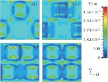
To validate the aforementioned analysis of the tunable absorption in the equivalent circuit model, simulations of the average E-field magnitude on the outer surface of the absorber are carried out. The incident E-field is perpendicular to the moving direction of the top FSS. With a displacement of 0 mm, 4 mm, 8 mm, and 11 mm respectively, simulation results at 8 GHz are shown in Fig. 5 and at 17 GHz in Fig. 6. The E-field in the coupling area between two FSSs is obviously stronger than the other area. The area with higher field intensity increases, corresponding to the increase of the moving distance of the top FSS, which means that the coupling capacitance between two FSSs also increases. In other words, the coupling capacitance is tunable along with the variation of the overlapping area between the two FSSs. This analytical result agrees well with the calculated circuit parameters derived from the results of full-wave simulations. A curve-fitting process is adopted to obtain the best fit between the equivalent circuit output and the full-wave response. The values of the intercoupling capacitance C12 varying with the movement distance of the top FSS are plotted in Fig. 7. So, the conclusion is easily obtained that the relative movements of two closely coupled FSS surfaces result in a tunable coefficient C12, which is responsible for the tunability of the absorber.
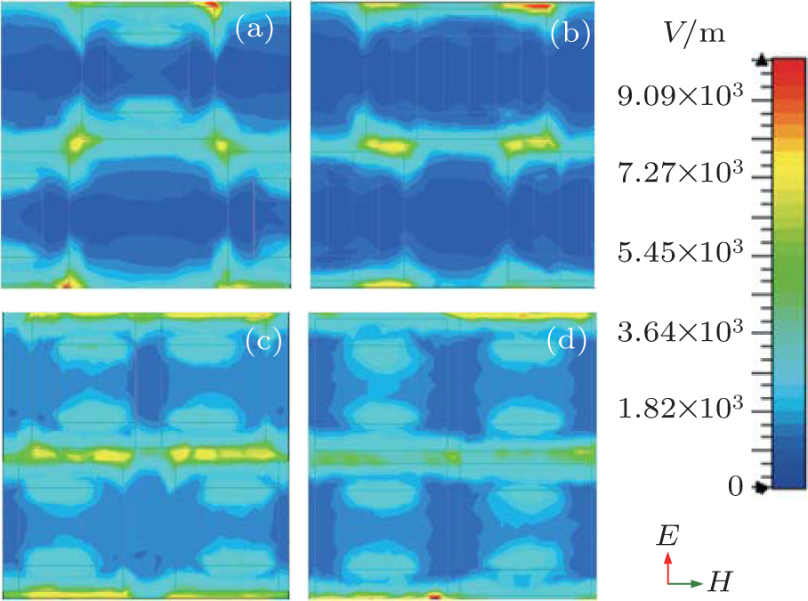 | Fig. 5. Electric field distributions on the outer surface of the absorber at 8 GHz when the top FSS has different displacements: (a) 0 mm, (b) 4 mm, (c) 8 mm, and (d) 11 mm. |
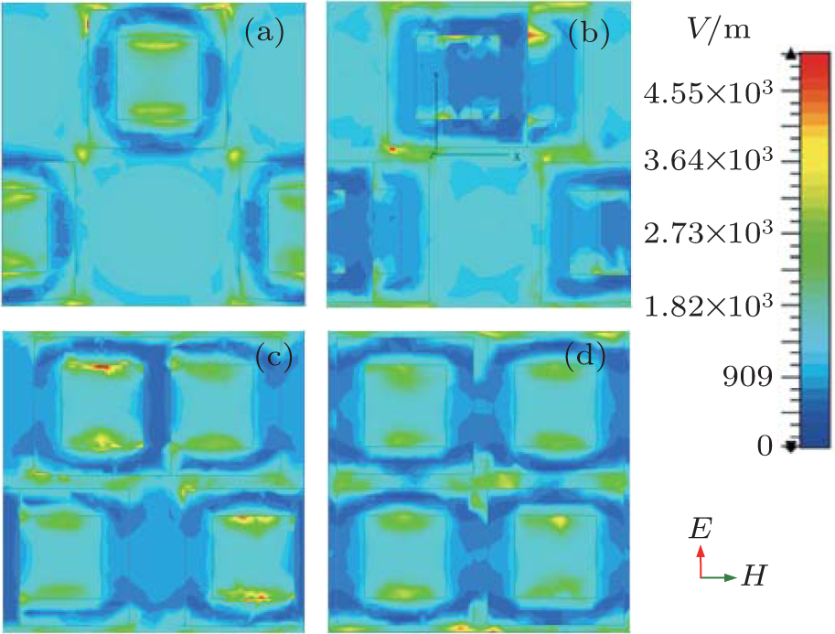 | Fig. 6. Electric field distributions on the outer surface of the absorber at 17 GHz when the top FSS has different displacements: (a) 0 mm, (b) 4 mm, (c) 8 mm, and (d) 11 mm. |
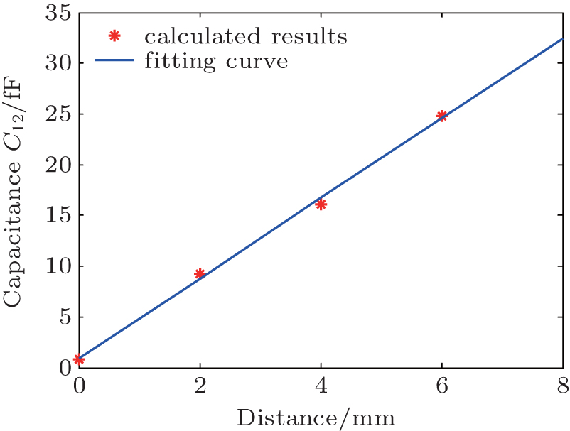 | Fig. 7. Variations of capacitance C12 with the movement distance of the top FSS. The other extracted circuit parameters for the proposed equivalent circuit model are R1 = 420 Ω , L1 = 4.88 nH, and C1 = 29.84 fF. |
Comparing the E-field magnitudes in Fig. 5 with those in Fig. 6, it is obvious that the resonance at 8 GHz is stronger than the resonance at 17 GHz (the ranges of the color mapping are different). They coincide with the simulated reflections in Fig. 4 which show that the absorption peak about 8 GHz is deeper than the other ones around 17 GHz. Besides, the strengths of the resonance are also quite different when the two FSSs have different relative movements. Generally, at the frequency of 8 GHz, the longer the top FSS moves, the weaker the resonance is. The situation at the frequency of 17 GHz is a little complicated. That is because the lattice period is larger than the wavelength at 17 GHz, which will result in high order diffractions.
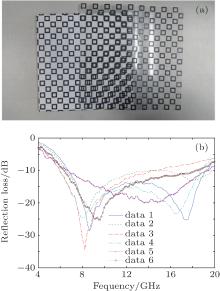
The tunable absorber structure is fabricated following the dimensions mentioned above (shown in Fig. 8(a)). In the sample, the resistive FSSs are fabricated by the silk printing technology, which is realized by printing carbonic conductive ink with a thickness of 25 μ m on separate substrates. The top FSS is printed on a piece of polyethylene terephthalate (PET) paper 50 μ m in thickness, so that it is moveable. The second FSS is directly printed on the dielectric layer which is a foam board with a thickness of d = 5 mm and with a permittivity of ɛ r = 1.13. A flat aluminum sheet is located below the foam, serving as a ground plane. To make the top layer attach to the substrate steadily but still movable, a little lubricant oil is spread between the PET film and the foam. Ultimately, the overall size of the experimental sample is 200 mm × 200 mm with a whole thickness of 5.1 mm.
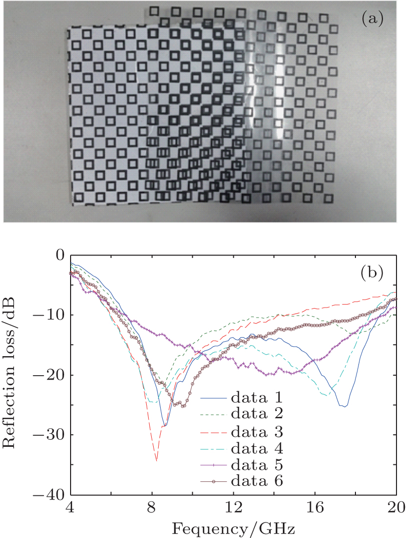 | Fig. 8. (a) Photograph of the experiment sample. (b) Measured reflection losses of the structure with different unit cells (the unit cells on the right are depicted partially with only the center). |
Using a two-port vector network analyzer and a pair of 2 GHz– 20 GHz horn antennas, which can supply a linearly polarized incident E-field parallel to the x axis of the absorber, reflection loss measurements are carried out in an anechoic chamber. We slightly pulled the top layer along the x or y direction in steps of 1 mm. Because of the periodicity of the FSS, the maximum distance moved in each direction should not be more than a periodic length.
Out of all the results, six typical lines of measured reflection loss as well as their corresponding patterns are plotted in Fig. 8(b). The results show good agreement between the simulation results and the experimental measurements. Concretely, though the frequencies of peak absorptions are different from each other, each line owns a bandwidth of active microwave absorbing within which the structure’ s reflectivity is always less than − 10 dB in a frequency range from 8.61 GHz to 13.13 GHz. The absorption peaks can be tuned, especially within two sub-bands (from 8.12 GHz to 9.50 GHz and from 14.86 GHz to 18.10 GHz). Anyhow we actually obtain a tunable and wideband absorber in a wide frequency range from 5.90 GHz to 19.73 GHz and its overall thickness is less than λ 0/4.
A novel structure that is based on the resistively loaded high impedance surface and with two layers of FSSs is proposed. By changing the composite unit cell pattern, the absorber not only exhibits the wideband microwave absorbing characteristic within a frequency bandwidth of nearly 14 GHz, but also is tunable in a range of 33% of the overall absorption band. The absorber exhibits three working modes which can satisfy different situations. It is anticipated that we are able to broaden the absorbing and tunable bandwidth by optimizing the design of the resistive FSS through using the complex element shapes with appropriate resistance.
| 1 |
|
| 2 |
|
| 3 |
|
| 4 |
|
| 5 |
|
| 6 |
|
| 7 |
|
| 8 |
|
| 9 |
|
| 10 |
|
| 11 |
|
| 12 |
|
| 13 |
|
| 14 |
|
| 15 |
|
| 16 |
|
| 17 |
|
| 18 |
|
| 19 |
|
| 20 |
|