†Corresponding author. E-mail: skyboyhj@163.com
*Project supported by the National Natural Science Foundation of China (Grant No. 61401430).
The linearity of the traveling-wave tube is a very important characteristic for a modern communication system. To improve the linearity of the traveling-wave tube at no expense of the saturated output power and overall efficiency, a modified pitch profile combined with a small adjustment of operating parameters is proposed. The optimal design of the helix circuit is evaluated theoretically by a large signal analysis, and the experimental test is also carried out to make a comparison of performance between the novel and original designed traveling-wave tubes. The experiments show that the saturated output powers and efficiencies of these two tubes are close to each other, while the linearity of the traveling-wave tube is obviously improved. The total phase shift and AM/PM conversion at saturation of the novel tube, averaged over the operating band, are only 30.6°/dB and 2.5°/dB, respectively, which are 20.1°/dB and 1.6°/dB lower than those of the original tube, respectively. Moreover, the third-order intermodulation of the novel tube is up to 2.2 dBc lower than that of the original tube.
The development of broadband digital satellite communications and other wireless data/communication networks places emphasis on the increasing demands for high power, broadband, highly linear and compact RF amplifiers.[1– 3] Compared with the solid state power amplifier (SSPA), the vacuum electronics amplifier has an excellent efficiency and can support much more active channels without driving the platform into unreliable high temperature ranges which are detrimental for other temperature-sensitive components. Owing to the combined high efficiency, bandwidth, power, and reliability, the vacuum electronics amplifier is still a preferable choice for applications in many terrestrial and space-based communications.
Multilevel, multiphase digital modulation schemes such as m-ary phase-shift keying (PSK) and quasi-constantenvelope (QPSK) modulations are required to possess the linear characteristic of communications amplifiers. A predistorter is commonly adapted in front of the traveling-wave tube (TWT) to improve the linearity, while the resulting linearized TWT shows a quicker drop of output power as a function of input back-off.[4] Operation “ back-off” from saturation improves the linearity but reduces the power and efficiency of TWT. This power reduction can have an influence on the communication link availability.[5, 6] Generally, TWT designers try to achieve desired power and linearity performances by balancing the helix circuit characteristics and efficiency optimization combined with output power back-off.[7, 8]
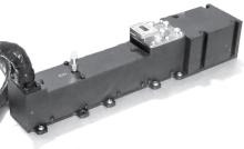
K-band TWTs with the merit of large available bandwidth are needed in larger quantities for the multimedia applications, thus shifting the market share to higher frequencies. We have developed the conduction-cooled K-band TWTs for space communications with high efficiency, bandwidth, and power at the Institute of Electronics, Chinese Academy of Sciences (IECAS) and the TWT is shown in Fig. 1. A four-stage axi-symmetric depressed collector was successfully designed and developed to reduce backward current and increase the overall efficiency for this space TWT.
In this paper, an improvement of the linearity of this K-band TWT at no expense of the saturated output power and efficiency is achieved. This helix circuit is subjected to various experimental tests.
The rest of this paper is organized as follows. In Section 2, the design strategy for the objective of linearity optimization is described. In Section 3, a large signal analysis of the tube is carried out over the operating band to theoretically evaluate the performance of the modified design. In Section 4, a tube of TWT2 is developed with a modified pitch profile taking the original pitch profile tube TWT1 as a baseline. The experimental results of the two tubes are compared to demonstrate the improved performance on linearity. Finally, some conclusions are drawn from the present study in Section 5.
An existing two-section K-band helix TWT, with the pitch profile designated as helix-1, is used as the baseline for design purpose. Helix SWS has a very wide bandwidth, which results from its low dispersion. The helix is supported by an insulating structure that takes the form of three equally spaced dielectric rods. A helix slow wave structure (SWS) with three T-shape supported rods as shown in Fig. 2(a) is used to obtain a flat dispersion relation, high impedance, and low RF loss. The materials of supported rods and helix are chosen as BN and molybdenum plated copper, respectively. To eliminate regenerative oscillations along the circuit and increase the stable gain, a sever and attenuator are introduced into the TWT. The attenuator design contains a continuous taper to provide a good match and a long section for sufficient attenuation. The loss of TWT along the axial length is shown in Fig. 2(b). This helix TWT is assembled with a four-stage collector, Sub-Miniature A (SMA) connector as an input and WR51 waveguide as an output. The operating voltage and beam current are 6.75 kV and 45 mA, respectively.
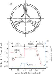 | Fig. 2. (a) Sketch of a section of SWS; (b) loss profile and different pitch profiles of the K-band TWT. |
A suite of accurate, physics-based helix TWT numerical design tools IESTWT is employed to optimize the linearity of TWT at no expense of the output power and interaction efficiency. As a three-dimensional (3D) multi-frequency largesignal model, IESTWT has been experimentally validated[9, 10] and has been proved to be effective for the parameter design.
The modified pitch profile helix-2 in Fig. 2(b) has three sections: input section, center section, and output section. The input section is divided into three parts: the first part is lower uniform pitch P1, the second part is positive taper, and the third part is uniform pitch P2. As is well known, with the decrease of helix pitch, the phase velocity of helix slows down, and the TWT could work at a lower operating voltage. By introducing the first lower pitch P1 followed by a positive taper, the operating voltage could be effectively reduced. As the phase of RF output varies with the operating voltage, [11] it is possible to reduce the phase shift of TWT by adopting this modified input section. As a full consideration of phase shift and basic efficiency, the helix pitch P1 should be chosen to lie in a range of 0.94P2 < P1 < 0.98P2. In addition, the pitch P2 of this section is chosen for maximum small-signal gain. The length of this section is chosen to give a gain of at least 20 dB in the input section to ensure that the growing wave is fully established.
The central section is the zone of positive phase compensation, of which the pitch P3 determines the coupling to the fast space-charge wave, and thus an amount of phase compensation is introduced. In this modified design of pitch profile, the pitch P3 is augmented to achieve greater interaction with the fast space-charge wave and an optimum electron bunch formation. However, if the pitch P3 is too large (P3 > 1.1P2), the synchronization condition for effective beam-wave interaction would be weakened and the basic efficiency would be distinctly reduced. Therefore, the increased amount of pitch P3 should be chosen properly as a compromise between phase compensation and interaction efficiency. The length of this section is adjusted to obtain maximum forward circuit power.
As an effective way to prevent the gain from decreasing and maintain the velocity parameter constant, the dynamic velocity taper (DVT) developed by Kosmahl and Peterson[12] is adopted to improve the linearity and output power in the output section. When the energy is repeatedly and cumulatively transferred from the electrons to the circuit, the TWT approaches to nonlinear operation. The average velocity of the beam and the velocity parameter decrease. DVT is an effective way to prevent the gain from decreasing and maintain the velocity parameter constant. The choice of the pitch for the output section is also conditioned by the efficiency versus phase shift compromise.[13] The helix pitches P4 and P5 of this section are chosen to be 1.01P2 and 0.91P2, respectively.
To evaluate the performance of the proposed TWT (TWT2) theoretically, a large signal analysis of the tube is carried out over the operating band at a cathode voltage of 6.5 kV and a beam current of 48 mA with an average beam fill factor of 50%. The operating parameters are slightly modified to achieve high linearity performance of TWT. A comparison of performance between TWT2 and TWT1 is performed to examine its improved property. The simulation results, including output powers, gain, nonlinear phase shifts, and AM– PM conversions of TWT1 and TWT2 at a central operating frequency f0 = 20.2 GHz are shown in Figs. 3 and 4, respectively.
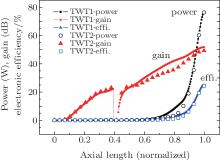 | Fig. 3. Comparisons of output power, gain, and electronic efficiency along axial length between TWT1 and TWT2. |
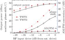 | Fig. 4. Comparisons of output power, nonlinear phase shift, and AM– PM conversion versus input power between TWT1 and TWT2. |
Figure 3 shows that the saturated output power, gain, and electronic efficiency of TWT1 are 77.1 W, 51.8 dB, and 25.4%, respectively, and those of TWT2 are 76.4 W, 49.3 dB, and 24.4%, respectively, indicating that the main properties of these two TWTs are similar. However, figure 4 illustrates that the nonlinear phase shift and maximum AM– PM conversion of TWT1 are 46.7° /dB and 3.49° /dB, respectively, while those of TWT2 are 27.5° /dB and 2.47° /dB, respectively. Therefore, the comparison suggests that the linearity of TWT can be significantly improved at no expense of the main properties by modifying the pitch profile and optimizing the operating parameters.
To validate the previous simulation results, a tube of TWT2 is developed with a pitch profile according to helix-2 with considering the pitch profile helix-1 tube of TWT1 as a baseline. The test operating voltage and current of TWT1 are 6.71 kV and 45.4 mA, while those of TWT2 are 6.45 kV and 47.8 mA. The experimental findings of TWT1 and TWT2 are presented in detail.
A comparison of the main property between TWT1 and TWT2 is shown in Fig. 5, where f0 is 20.2 GHz. The saturated output power and basic efficiency of TWT2 are higher than those of TWT1 in a frequency range of f > f0.
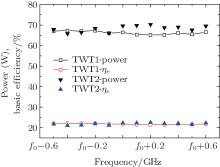 | Fig. 5. Comparisons of experimental saturated output power and basic efficiency between TWT1 and TWT2. |
The linearity of space TWT usually includes the nonlinear phase shift, amplitude modulation-to-phase modulation (AM-to-PM) conversion, and carrier-to-third-order-intermodulation (C/3IM) separation. An experimental comparison between TWT1 and TWT2 in the aspects of these three parameters is performed to validate the improved linearity of TWT2.
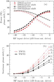
The experimental results of nonlinear phase shift are given in Figs. 6(a) and 6(b). The curves of output power and phase shift versus input power of TWT1 and TWT2 are shown in Fig. 6(a), where the intermediate frequency (IF) bandwidth of the vector network analyzer is set to be 20 Hz. Compared with TWT1, TWT2 has higher output power and obviously lower phase shift. Figure 6(b) depicts the comparisons of phase shift versus input power across the operating frequency band between TWT1 and TWT2, where f1 = f0 − 0.5 GHz, f2 = f0 + 0.6 GHz. The phase shifts at input powers of 0, − 3, − 6, − 9, − 12, and − 15 dB relative to saturation of TWT2 are 29.2° , 21.7° , 14.7° , 8.1° , 3.0° , and 0.04° , respectively, which are obviously less than those of TWT1. The nonlinear phase shifts of TWT2 at f1, f0, and f2 are 25.1° , 29.2° , and 37.6° , respectively, which are 42.2%, 41.7%, and 31.1% lower than those of TWT1.
As a common merit for space TWTs, AM-to-PM conversion is a measure of the phase modulation imparted to a carrier by a neighboring amplitude-modulated carrier. Figure 7 gives the AM/PM conversion curves of TWT1 and TWT2 across the operating frequency band, obtained by calculating the derivative of phase shift versus power. The maximum values of AM/PM conversion of TWT2 at f1, f0, and f2 are 2.17° /dB, 2.48° /dB, and 3.11° /dB, respectively. Meanwhile, the AM/PM conversion at input powers of 0, − 3, − 6, − 9, and − 12 dB relative to saturation of TWT2 are 2.48° /dB, 2.33° /dB, 2.21° /dB, 1.70° /dB, and 0.99° /dB, respectively, which are 31% on average lower than those of TWT1.
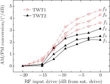 | Fig. 7. Comparison of experimental AM/PM conversion versus input power across the operating frequency band between TWT1 and TWT2. |
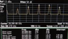
Intermodulation (IM) occurs when two or more carrier signals are amplified by a TWT. The third-order intermodulation is most important because it is closest to the signal frequency and has the largest amplitude. Figure 8 shows the experimental results of third-order IM, obtained by spectrum analyzer. The input frequencies are f0 and f0 + 5 MHz, and the ratio between the video bandwidth and the resolution bandwidth (VBW/RBW) is 3× 10− 4 with a span of 30 MHz. The difference between the amplitudes at the two main frequencies is only 0.05 dBc. Table 1 depicts the comparison of C/3IM versus input power across the operating frequency band between TWT1 and TWT2. The C/3IM at input powers of − 3, − 6, − 9, and − 12 dB relative to saturation of TWT2 are − 10.44, − 12.46, − 15.21, and − 18.2 dBc, respectively, which are 1 dBc– 2.2 dBc less than those of TWT1. Moreover, when input power per carrier is − 3 dB relative to single carrier saturation, the C/3IM values of TWT2 at f1, f0, and f2 are − 10.8, − 10.44, and − 10.33 dBc, respectively, which are distinctly lower than those of TWT1. By adopting pitch profile helix-2, the gain compression and phase shift of TWT2 are reduced, and thus the I3M is accordingly reduced.
| Table 1. Experimental C/3IM results across the operating frequency band between TWT1 and TWT2. |
Based on the existing two-section millimeter wave helix TWT at IECAS, a modified pitch profile combined with a small adjustment of operating parameters is investigated to improve the linearity of TWT. The optimal design of the helix circuit is evaluated theoretically and is also validated experimentally. From the comparison of performance between the optimized and original designed TWTs, it follows that the total phase shift, AM/PM conversion, and C/3IM of TWT2 are obviously lower than those of TWT1, while the saturated output powers and overall efficiencies of both of these two tubes are similar. It can thus be concluded that increasing the linearity of K-band TWT at no expense of output power and efficiency is feasible.
| 1 |
|
| 2 |
|
| 3 |
|
| 4 |
|
| 5 |
|
| 6 |
|
| 7 |
|
| 8 |
|
| 9 |
|
| 10 |
|
| 11 |
|
| 12 |
|
| 13 |
|


