| INTERDISCIPLINARY PHYSICS AND RELATED AREAS OF SCIENCE AND TECHNOLOGY |
Prev
Next
|
|
|
New embedded DDSCR structure with high holding voltage and high robustness for 12-V applications |
| Jie-Yu Li(李婕妤)1,2, Yang Wang(汪洋)1,2,†, Dan-Dan Jia(夹丹丹)1,2, Wei-Peng Wei(魏伟鹏)1,2, and Peng Dong(董鹏)3 |
1 School of Physics and Optoelectronics, Xiangtan University, Xiangtan 411105, China
2 Hunan Engineering Laboratory for Microelectronics, Optoelectronics and System on A Chip, Xiangtan 411105, China
3 SuperESD Microelectronics Technology CO., LTD., Changsha 410100, China |
|
|
|
|
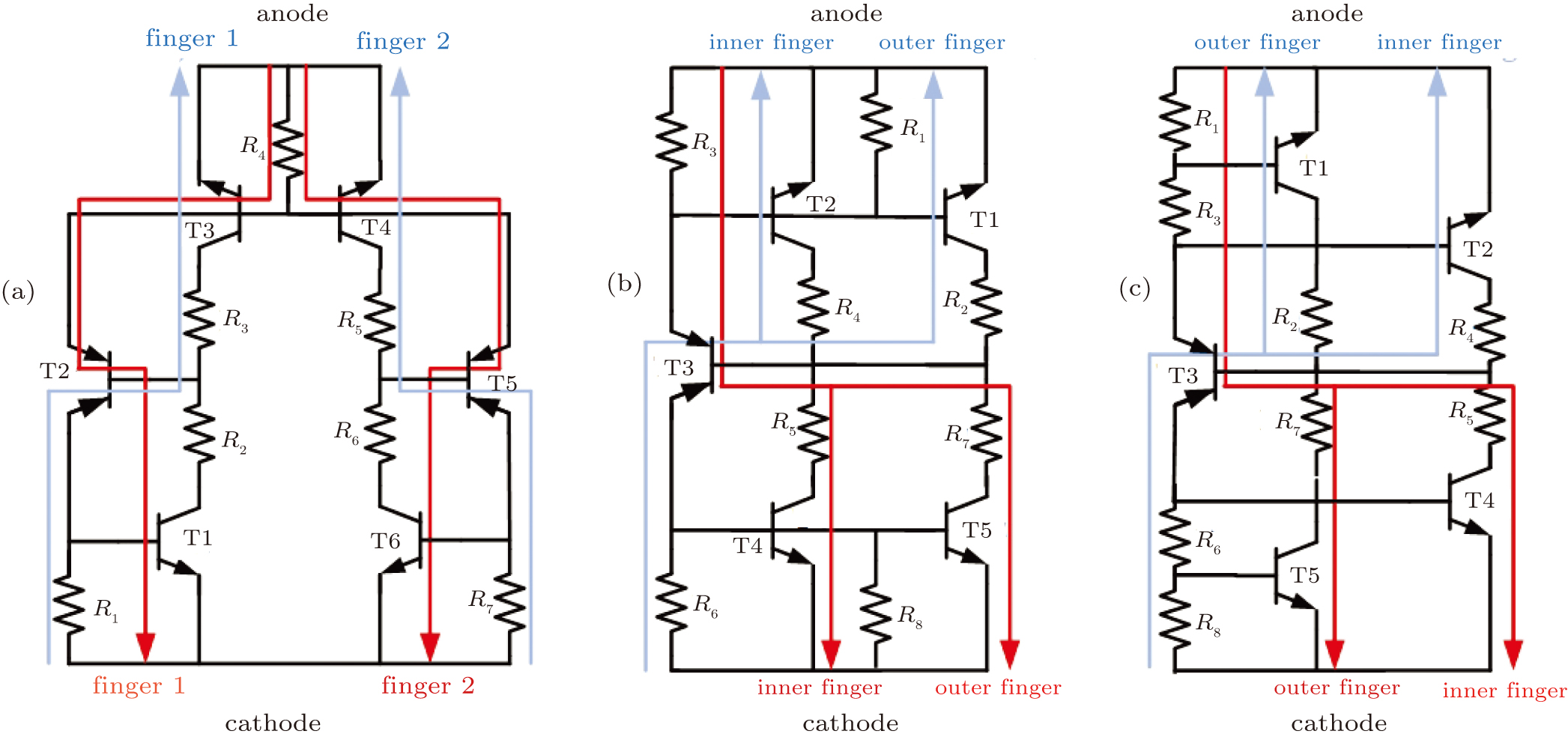
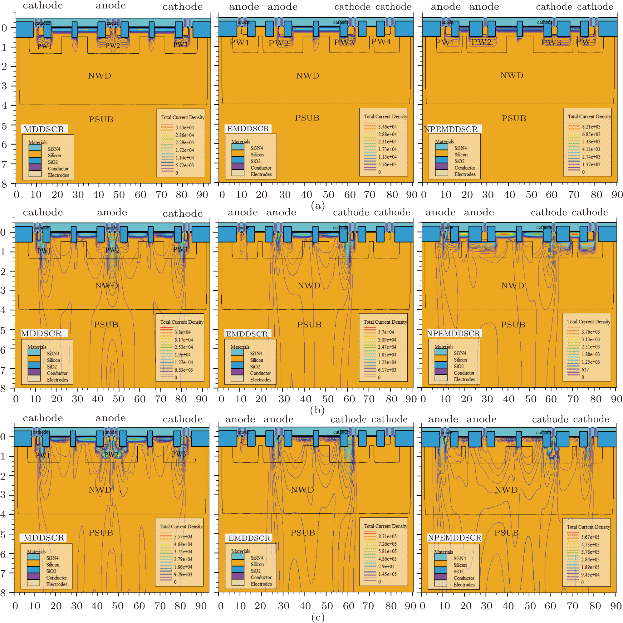
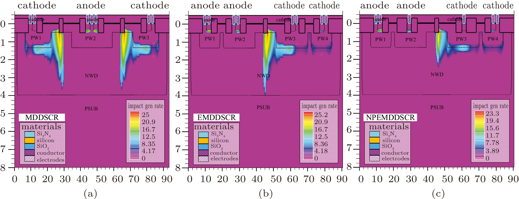
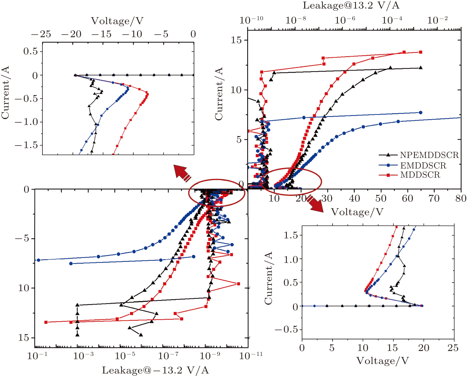
Abstract A new dual directional silicon-controlled rectifier based electrostatic discharge (ESD) protection device suitable for 12-V applications is proposed in this paper. The proposed device (NPEMDDSCR) is based on the embedded DDSCR (EMDDSCR) structure, in which the P+ electrode and P+ injection are removed from the inner finger. Compared with the conventional modified DDSCR (MDDSCR), its high holding voltage meets the requirements for applications. Compared with the embedded DDSCR (EMDDSCR), it has good conduction uniformity. The MDDSCR, EMDDSCR, and NPEMDDSCR are fabricated with an identical width in a 0.5-μm CDMOS process. In order to verify and predict the characteristics of the proposed ESD protection device, a transmission line pulse (TLP) testing system and a two-dimensional device simulation platform are used in this work. The measurements demonstrate that the NPEMDDSCR provides improved reliability and higher area efficiency for 12 V or similar applications. The measurement results also show that the NPEMDDSCR provides higher robustness and better latch-up immunity capability.
|
Received: 09 May 2020
Revised: 12 June 2020
Accepted manuscript online: 23 June 2020
|
|
PACS:
|
85.30.De
|
(Semiconductor-device characterization, design, and modeling)
|
| |
85.30.Rs
|
(Thyristors)
|
| |
73.40.Lq
|
(Other semiconductor-to-semiconductor contacts, p-n junctions, and heterojunctions)
|
|
|
Corresponding Authors:
†Corresponding author. E-mail: wangyang@xtu.edu.cn
|
| About author: †Corresponding author. E-mail: wangyang@xtu.edu.cn * Project supported by the National Natural Science Foundation of China (Grant Nos. 61704145, 61774129, and 61827812), the Natural Science Foundation of Hunan Province, China (Grant No. 2019JJ50609), and the Key Technology Program of Changsha City, China (Grant No. kq1902042). |
Cite this article:
Jie-Yu Li(李婕妤), Yang Wang(汪洋)†, Dan-Dan Jia(夹丹丹), Wei-Peng Wei(魏伟鹏), and Peng Dong(董鹏) New embedded DDSCR structure with high holding voltage and high robustness for 12-V applications 2020 Chin. Phys. B 29 108501
|
| [1] |
|
| [2] |
|
| [3] |
Wang Y, Jin X L 2019 IEEE 26th International Symposium on Physical and Failure Analysis of Integrated Circuits July, 2019 Hangzhou, China DOI: 10.1109/IPFA47161.2019.8984875 |
| [4] |
|
| [5] |
|
| [6] |
|
| [7] |
Liu Z W, He J, Liu J J, Liu J Z, Miao M, Dong S R 2012 IEEE Solid-State and Integrated Circuit Technology October, 2012 Xi’an, China DOI: 10.1109/ICSICT.2012.6467917 |
| [8] |
Huang X Z, Liu J J, Liu Z W, Liu F, Liu J Z, Cheng H 2016 IEEE Electron Dev. Lett. 37 1311 DOI: 10.1109/LED.2016.2598063 |
| [9] |
|
| [10] |
|
| [11] |
|
| [12] |
Huo M X, Ding K B, Han Y, Dong S R, Du X Y, Huang D H, Song B 2009 16th IEEE International Symposium on the Physical and Failure Analysis of Integrated Circuits July, 2009 Suzhou, China DOI: 10.1109/IPFA.2009.5232711 |
| [13] |
Wang Y, Jia D D, Chen X J, Jin X L 2019 IEEE 26th International Symposium on Physical and Failure Analysis of Integrated Circuits July, 2019 Hangzhou, China DOI: 10.1109/IPFA47161.2019.8984915 |
| No Suggested Reading articles found! |
|
|
Viewed |
|
|
|
Full text
|
|
|
|
|
Abstract
|
|
|
|
|
Cited |
|
|
|
|
Altmetric
|
|
blogs
Facebook pages
Wikipedia page
Google+ users
|
Online attention
Altmetric calculates a score based on the online attention an article receives. Each coloured thread in the circle represents a different type of online attention. The number in the centre is the Altmetric score. Social media and mainstream news media are the main sources that calculate the score. Reference managers such as Mendeley are also tracked but do not contribute to the score. Older articles often score higher because they have had more time to get noticed. To account for this, Altmetric has included the context data for other articles of a similar age.
View more on Altmetrics
|
|
|