| CONDENSED MATTER: ELECTRONIC STRUCTURE, ELECTRICAL, MAGNETIC, AND OPTICAL PROPERTIES |
Prev
Next
|
|
|
Short-wavelength infrared InAs/GaSb superlattice hole avalanche photodiode |
| Jia-Feng Liu(刘家丰)1,2, †, Ning-Tao Zhang(张宁涛)4, †, Yan Teng(滕)1,2, Xiu-Jun Hao(郝修军)2,3, Yu Zhao(赵宇)2, Ying Chen(陈影)1,2, He Zhu(朱赫)1,2, Hong Zhu(朱虹)1,2, Qi-Hua Wu(吴启花)2, Xin Li(李欣)2, Bai-Le Chen(陈佰乐)4,§, and Yong Huang(黄勇)1,2,, ‡ |
1 School of Nano-Tech and Nano-Bionics, University of Science and Technology of China, Hefei 230026, China
2 Key Laboratory of Nanodevices and Applications, Suzhou Institute of Nano-Tech and Nano-Bionics, Chinese Academy of Sciences, Suzhou 215123, China
3 School of Physical Science and Technology, ShanghaiTech University, Shanghai 201210, China
4 School of Information Science and Technology, ShanghaiTech University, Shanghai 201210, China |
|
|
|
|
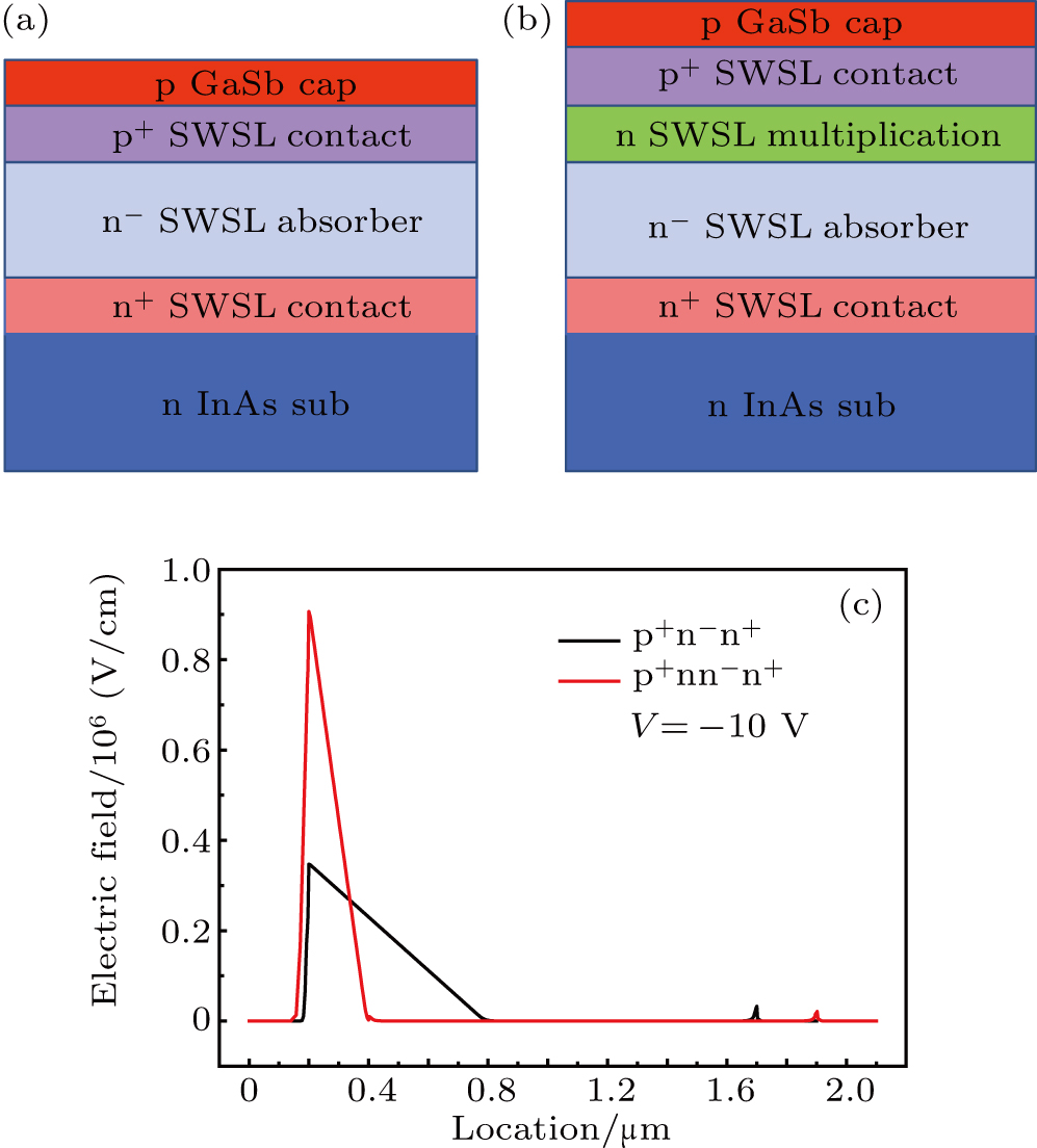
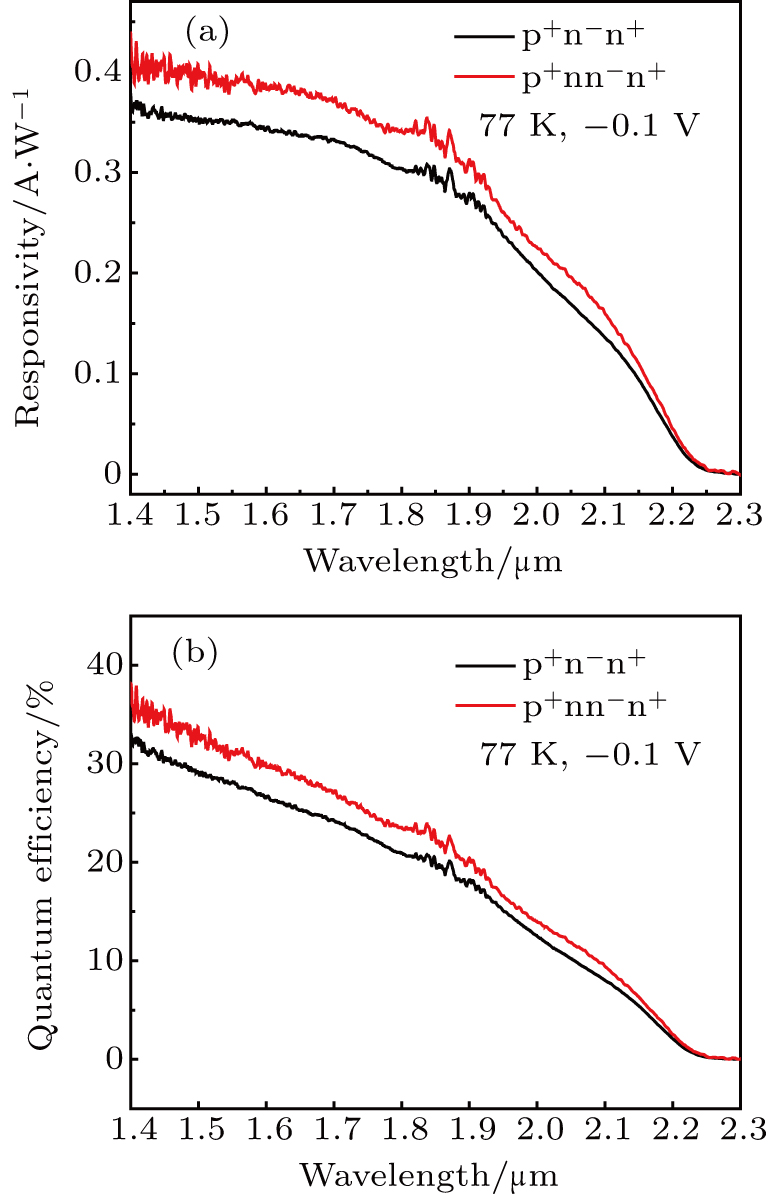
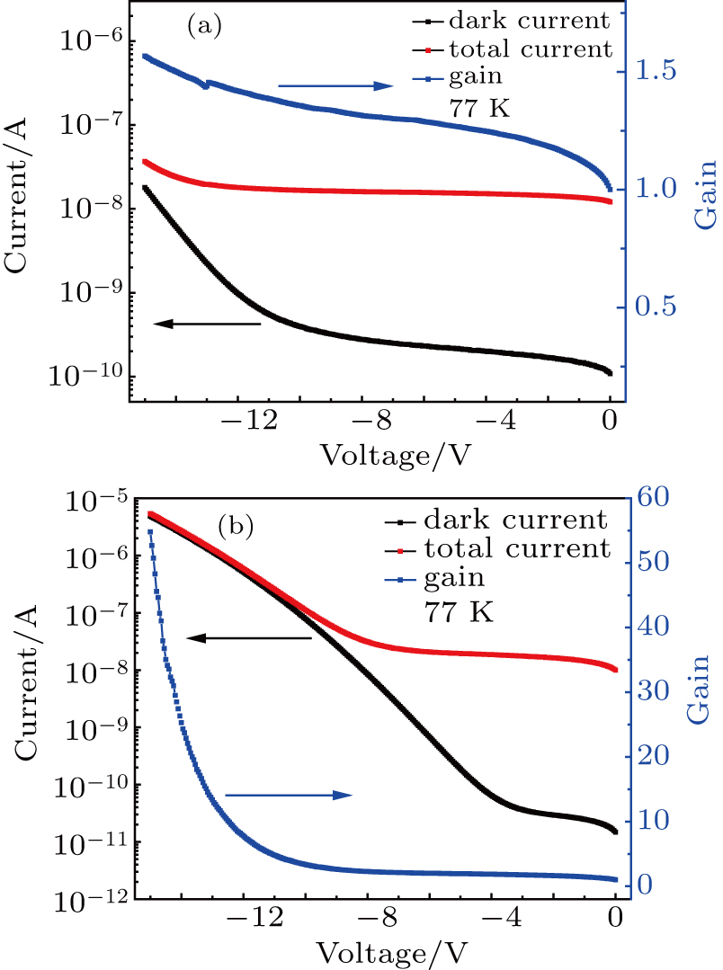
Abstract We demonstrate two short-wavelength infrared avalanche photodiodes based on InAs/GaSb superlattice grown by metal-organic chemical vapor deposition. The difference between the two devices, namely, p+n−n+ and p+nn−n+, is that the p+nn−n+ device possesses an additional middle-doped layer to separate the multiplication region from the absorption region. By properly controlling the electric field distribution in the p+nn−n+ device, an electric field of 906 kV/cm has been achieved, which is 2.6 times higher than that in the p+n−n+ device. At a reverse bias of –0.1 V at 77 K, both devices show a 100% cut-off wavelength of 2.25 μm. The p+n−n+ and p+nn−n+ show a dark current density of 1.5 × 10⁻⁷ A/cm2 and 1.8 × 10⁻⁸ A/cm2, and a peak responsivity about 0.35 A/W and 0.40 A/W at 1.5 μm, respectively. A maximum multiplication gain of 55 is achieved in the p+nn−n+ device while the value is only less than 2 in the p+n−n+ device. Exponential nature of the gain characteristic as a function of reverse bias confirms a single carrier hole dominated impact ionization.
|
Received: 13 May 2020
Revised: 19 June 2020
Accepted manuscript online: 06 July 2020
|
| Fund: the National Natural Science Foundation of China (Grant Nos. 61874179, 61804161, and 61975121) and the National Key Research and Development Program of China (Grant No. 2019YFB2203400). |
|
Corresponding Authors:
†These authors contributed equally to this work. ‡Corresponding author. E-mail: yhuang2014@sinano.ac.cn §Corresponding author. E-mail: chenbl@shanghaitech.edu.cn
|
Cite this article:
Jia-Feng Liu(刘家丰), Ning-Tao Zhang(张宁涛), Yan Teng(滕), Xiu-Jun Hao(郝修军), Yu Zhao(赵宇), Ying Chen(陈影), He Zhu(朱赫), Hong Zhu(朱虹), Qi-Hua Wu(吴启花), Xin Li(李欣), Bai-Le Chen(陈佰乐)§, and Yong Huang(黄勇) Short-wavelength infrared InAs/GaSb superlattice hole avalanche photodiode 2020 Chin. Phys. B 29 117301
|
| [1] |
|
| [2] |
|
| [3] |
|
| [4] |
Banerjee K, Mallick S, Ghosh S, Plis E, Rodriguez J B, Krishna S, Grein C 2008 Mater. Res. Soc. Proc. 1076 1076-K02 DOI: 10.1557/PROC-1076-K02-02 |
| [5] |
Mallick S, Banerjee K, Ghosh S, Plis E, Rodriguez J B, Krishna S, Grein C 2007 Appl. Phys. Lett. 91 241111 DOI: 10.1063/1.2817608 |
| [6] |
Banerjee K, Ghosh S, Mallick S, Plis E, Krishna S, Grein C 2009 Appl. Phys. Lett. 94 201107 DOI: 10.1063/1.3139012 |
| [7] |
Nishida K, Taguchi K, Matsumoto Y 1979 Appl. Phys. Lett. 35 251 DOI: 10.1063/1.91089 |
| [8] |
|
| [9] |
Hoffman D, Nguyen B M, Delaunay P Y, Hood A, Razeghi M, Pellegrino J 2007 Appl. Phys. Lett. 91 143507 DOI: 10.1063/1.2795086 |
| [10] |
Yang Q K, Fuchs F, Schmitz J, Pletschen W 2002 Appl. Phys. Lett. 81 4757 DOI: 10.1063/1.1529306 |
| [11] |
|
| [12] |
Chen Y, Liu J F, Zhao Y, Teng Y, Hao X J, Li X, Zhu H, Zhu H, Wu Q H, Huang Y 2020 Infrared. Phys. Techn. 105 103209 DOI: 10.1016/j.infrared.2020.103209 |
| [13] |
|
| [14] |
Beck J, Wan C, Kinch M, Robinson J, Mitra P, Scritchfield R, Ma F, Campbell J 2006 J. Electron. Mater. 35 1166 DOI: 10.1007/s11664-006-0237-3 |
| [15] |
Ghosh S, Mallick S, Banerjee K, Grein C, Velicu S, Zhao J, Silversmith D, Rodriguez J B, Plis E, Krishna S 2008 J. Electron. Mater. 37 1764 DOI: 10.1007/s11664-008-0542-0 |
| No Suggested Reading articles found! |
|
|
Viewed |
|
|
|
Full text
|
|
|
|
|
Abstract
|
|
|
|
|
Cited |
|
|
|
|
Altmetric
|
|
blogs
Facebook pages
Wikipedia page
Google+ users
|
Online attention
Altmetric calculates a score based on the online attention an article receives. Each coloured thread in the circle represents a different type of online attention. The number in the centre is the Altmetric score. Social media and mainstream news media are the main sources that calculate the score. Reference managers such as Mendeley are also tracked but do not contribute to the score. Older articles often score higher because they have had more time to get noticed. To account for this, Altmetric has included the context data for other articles of a similar age.
View more on Altmetrics
|
|
|