| CONDENSED MATTER: ELECTRONIC STRUCTURE, ELECTRICAL, MAGNETIC, AND OPTICAL PROPERTIES |
Prev
Next
|
|
|
Surface termination effects on the electrical characteristics of La2O3/Al2O3 nanolaminates deposited by atomic layer deposition |
| Ji-Bin Fan(樊继斌)1, †, Shan-Ya Ling(凌山雅)1, Hong-Xia Liu(刘红侠)2, Li Duan(段理)1, Yan Zhang(张研)1, Ting-Ting Guo(郭婷婷)1, Xing Wei(魏星)1, and Qing He(何清)1$ |
1 School of Materials Science and Engineering, Chang’an University, Xi’an 710061, China
2 School of Microelectronics, Key Laboratory of Wide Band-Gap Semiconductor Materials and Devices, Xidian University, Xi’an 710071, China |
|
|
|
|
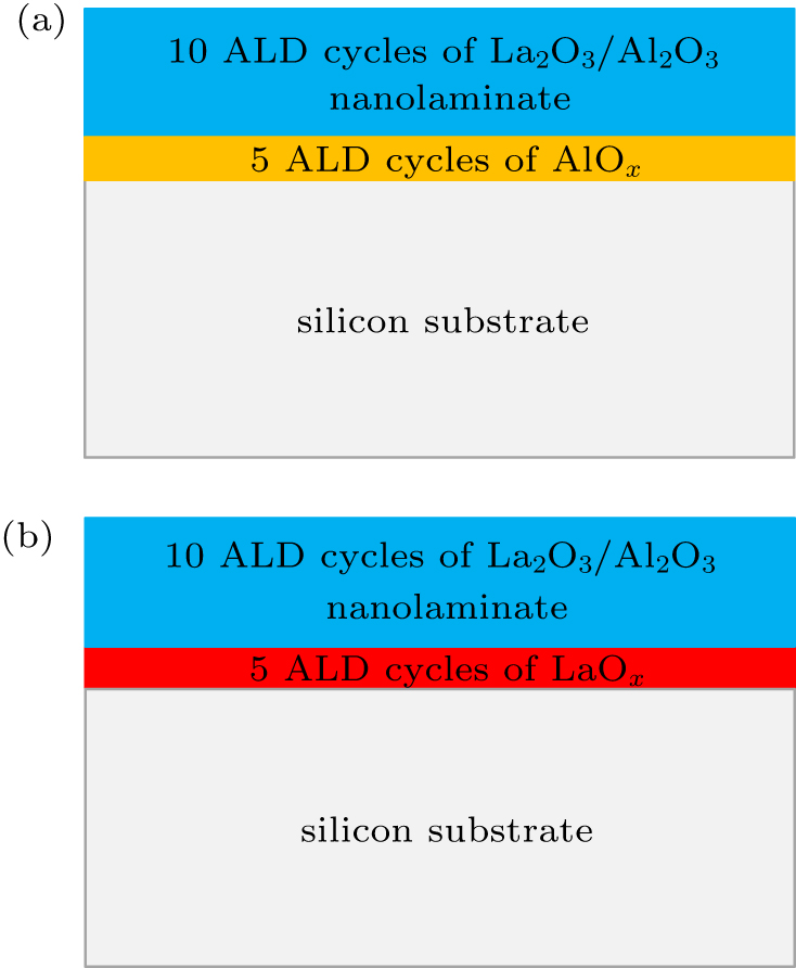
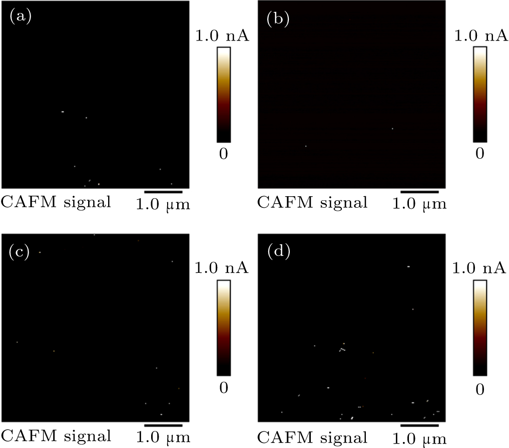
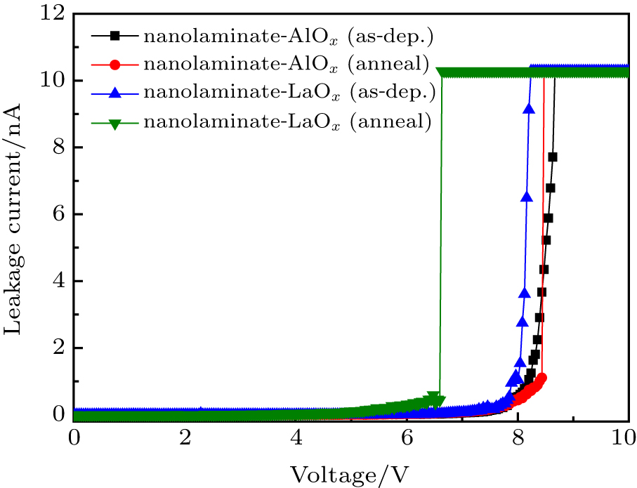
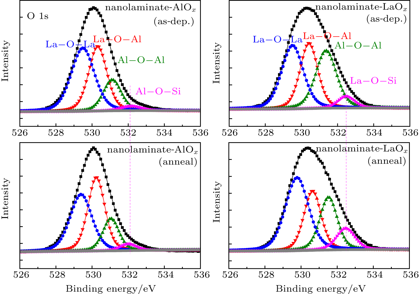
Abstract Effects of initial surface termination on electrical characteristics of La2O3/Al2O3 nanolaminates deposited by atomic layer deposition are studied by conductive atomic force microscopy working in contact mode and standard electrical characterization methods. It is found that, compared with La2O3/Al2O3 nanolaminates with LaOx as termination, lower interface trap density, less current leakage spots, and higher breakdown voltage are obtained in the La2O3/Al2O3 nanolaminates with AlOx as termination after annealing. A clear promotion of interface silicate layer is observed for La2O3/Al2O3 nanolaminates with AlOx as termination compared with LaOx as termination under the same annealing condition. In addition, the current conduction mechanism in La2O3/Al2O3 nanolaminates is considered as the Poole–Frenkel conduction. All results indicate that the AlOx is a more appropriate termination to deposit La2O3/Al2O3 nanolaminates on Si substrate, which is useful for the high-κ process development.
|
Received: 14 May 2020
Revised: 24 September 2020
Accepted manuscript online: 14 October 2020
|
| Fund: the National Natural Science Foundation of China (Grant Nos. 61604016 and 51802025), China Postdoctoral Science Foundation (Grant No. 2017M613028), the Fundamental Research Funds for the Central Universities, China (Grant Nos. 300102319209 and 300102310501) and the Innovation, and Entrepreneurship Training Program for Undergraduates (Grant Nos. 202010710231 and 201910710564). |
|
Corresponding Authors:
†Corresponding author. E-mail: jbfan@chd.edu.cn
|
Cite this article:
Ji-Bin Fan(樊继斌), Shan-Ya Ling(凌山雅), Hong-Xia Liu(刘红侠), Li Duan(段理), Yan Zhang(张研), Ting-Ting Guo(郭婷婷), Xing Wei(魏星), and Qing He(何清)$ Surface termination effects on the electrical characteristics of La2O3/Al2O3 nanolaminates deposited by atomic layer deposition 2020 Chin. Phys. B 29 117701
|
| [1] |
Gupta S, Gong X, Zhang R, Yeo Y C, Takagi S, Saraswat K C 2014 MRS Bull. 39 678 DOI: 10.1557/mrs.2014.163 |
| [2] |
Ablat A, Mamat M, Ghupur Y, Aimidula A, Wu R, Ali Baqi M, Gholama T, Wang J, Qian H, Wu R, Ibrahim W 2017 Mater. Lett. 191 97 DOI: 10.1016/j.matlet.2016.12.137 |
| [3] |
Mcdaniel M D, Ngo T Q, Hu S, Posadas A, Demkov A A, Ekerdt J G 2015 Appl. Phys. Rev. 2 041301 DOI: 10.1063/1.4934574 |
| [4] |
Fan J B, Liu H X, Li D L, Wang S L, Duan L, Yu X C 2017 J. Mater. Sci.: Mater. Electron. 28 11253 DOI: 10.1007/s10854-017-6914-6 |
| [5] |
Fujitsuka R, Sakashita M, Sakai A, Ogawa M, Yasuda Y 2005 Jpn. J. Appl. Phys. 44 2428 DOI: 10.1143/JJAP.44.2428 |
| [6] |
|
| [7] |
|
| [8] |
Kim L H, Kim K, Park S, Jeong Y J, Kim H, Chung D S, Kim S H, Park CE 2014 ACS Appl. Mater. Interfaces 6 6731 DOI: 10.1021/am500458d |
| [9] |
Werner F, Veith B, Zielke D, Kühnemund L, Tegenkamp C, Michael Seibt, Brendel1 R, Schmidt J 2011 J. Appl. Phys. 109 113701 DOI: 10.1063/1.3587227 |
| [10] |
Goncharova L V, Dalponte M, Feng T, Gustafsson T, Garfunkel E, Lysaght P S, Bersuker G 2011 Phys. Rev. B 83 115329 DOI: 10.1103/PhysRevB.83.115329 |
| [11] |
|
| [12] |
Mistry K, Allen C, Auth C, Beattie B, Bergstrom D, Bost M, Brazier M, Buehler M, Cappellani A, Chau R, Choi C H, Ding G, Fischer K, Ghani T, Grover R, Han W, Hanken D, Hattendorf M, He J, Zawadzki K 2007 Int. Electron Devices Meet. 247 DOI: 10.1109/IEDM.2007.4418914 |
| [13] |
Iwamoto K, Kamimuta Y, Ogawa A, Iwamoto K, Kamimuta Y, Arito Ogawa, Watanabe Y, Migita S, Mizubayashi W, Morita Y, Takahashi M, Ota H, Nabatame T, Toriumi A 2008 Appl. Phys. Lett. 92 132907 DOI: 10.1063/1.2904650 |
| [14] |
Min K H, Choi S, Jeong M S, Kang M G, Park S, Song H E, Lee J I, Kim D W 2019 Curr. Appl. Phys. 19 155 DOI: 10.1016/j.cap.2018.09.004 |
| [15] |
Matsuoka R, Shigesawa E, Miyamoto S, Sawano K, Itoh K M 2019 Semicond. Sci. Tech. 34 014004 DOI: 10.1088/1361-6641/aaf19b |
| [16] |
|
| [17] |
Vogel E M, Henson W K, Richter C A, Suehle J S 2000 IEEE T. Electron. Dev. 47 601 DOI: 10.1109/16.824736 |
| [18] |
|
| [19] |
|
| [20] |
Molina J, Tachi K, Kakushima K, Ahmet P, Hiroshi I 2006 ECS Trans. 3 233 DOI: 10.1149/1.2355715 |
| [21] |
Eom D, Hwang C S, Kim H J, Cho M H, Chung K B 2008 Electrochem. Solid-State Lett. 11 G33 DOI: 10.1149/1.2916437 |
| [22] |
Couso C, Iglesias V, Porti M, Claramunt S, Nafria M, Domingo N, Cordes A, Bersuker G 2016 IEEE Electron Dev. Lett. 37 640 DOI: 10.1109/LED.2016.2537051 |
| [23] |
Rao P K, Park B, Lee S T, Noh Y K, Kim M D, Oh J E 2011 J. Appl. Phys. 110 013716 DOI: 10.1063/1.3607245 |
| [24] |
|
| [25] |
|
| [26] |
Lin L I, Tang Z, Sun W, Wang P 1999 J. Mater. Sci. Tech. 15 439
|
| [27] |
|
| No Suggested Reading articles found! |
|
|
Viewed |
|
|
|
Full text
|
|
|
|
|
Abstract
|
|
|
|
|
Cited |
|
|
|
|
Altmetric
|
|
blogs
Facebook pages
Wikipedia page
Google+ users
|
Online attention
Altmetric calculates a score based on the online attention an article receives. Each coloured thread in the circle represents a different type of online attention. The number in the centre is the Altmetric score. Social media and mainstream news media are the main sources that calculate the score. Reference managers such as Mendeley are also tracked but do not contribute to the score. Older articles often score higher because they have had more time to get noticed. To account for this, Altmetric has included the context data for other articles of a similar age.
View more on Altmetrics
|
|
|